Table of Contents
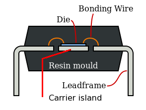
A typical PDIP:
Die
Part that has the actual active circuitry on it. Typically a few mm thick and can vary considerably in length and width. Most are rectangular in shape. This is a very complex part made of primarily silicon and silicon dioxide (SiO2), but also including aluminium, copper, arsenic, phosphorus, and more.
Resin mould
Its purpose is to protect the fragile die contained within. This includes physical stress and chemical stress such as moisture. On more advanced chips, it may also provide radiation protection or protections against reverse engineering. Typically an epoxy resin mixed with various additives such as glass.
Leadframe
Leads to provide a strong external connection to the internal circuitry.
The center portion is called by many names. Some of them include:
- Paddle (as found in US patent 7638862)
- Die mounting paddle [Plastic MEMS 68]
- Carrier island (eg by Beck's failure analysis)
- Mounting surface (as found in US patent 5610437)
- Die attach pad (as found here)
- Ceramic chip has “gold backing” and “bonding pad” here
As Beck's failure analysis is a well written published work I originally referred to it as a “carrier island.” However, die attach paddle or simply “paddle” seems to be the most common so I've standardized on that.
Bonding wire
Thin, usually gold, wires to electrically connect the leadframe to the die. For more details see the article on wire bonding.
Types
References
- Study and characterization of plastic encapsulated packages for MEMS (Plastic MEMS): http://www.wpi.edu/Pubs/ETD/Available/etd-01145-144711/unrestricted/thesis-final.pdf
