Table of Contents
Introduction
While this is not technically wire bonding since no wire is involved, it is a very common packaging method for modern high-density devices due to its improved thermal performance (heatsinks can be applied directly to the back side of the die).
Unlike normal wire bonding, in which the component side of the die faces up, a flip-chip package has the component side facing down. Solder bumps are applied directly to the bond pads. Flip-chip packages are almost universally BGAs (though some older CPUs were flip-chip pin grid array packages) and can be divided into two main subcategories:
Chip-scale packaging
Generally used for extremely high density devices but doesn't scale well to high pin counts due to the massive number of PCB layers and tiny vias that would be needed. The solder-bumped die is used directly as the finished device, possibly with some plastic applied to the back and between balls for protection.
Most commonly seen in flash and DRAM products.
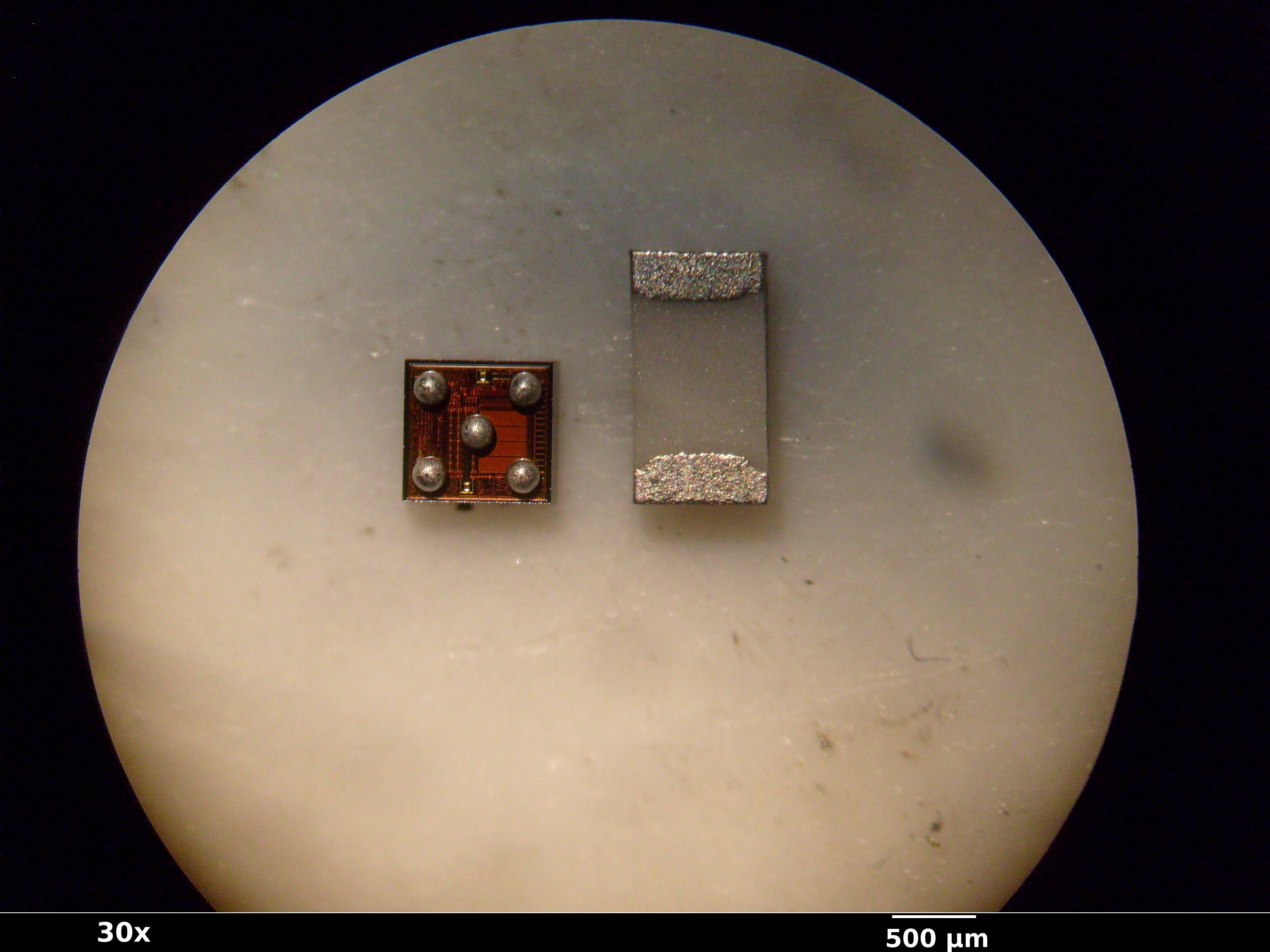
Example (Microchip 24AA16 EEPROM in 5-ball chip-scale package next to surface-mount resistor)
Breakout packages
The die is bumped with special high-temperature solder and soldered in the factory to a breakout board, which is a high-density multilayer PCB (often using microvias and extremely fine traces) that connects the fine-pitch solder bumps to a coarser-pitch BGA or PGA package compatible with standard printed circuit board processes.


