This is an old revision of the document!
Table of Contents
Active area
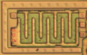
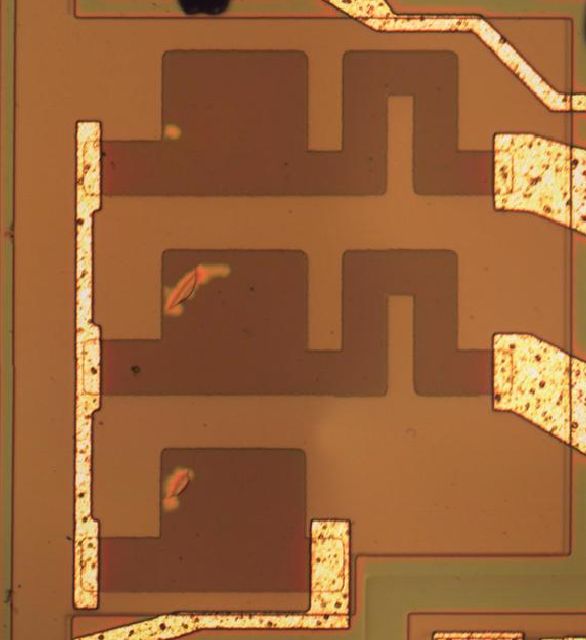
One common way to form resistors is to lay out one type of active area (ex: p) inside of another (ex: n) in a thin strip. Then reverse bias the junction to increase the resistance by shrinking the conductive area within the inner region. Example: (ST 24C02):
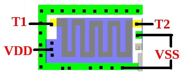
Which translates into:
I've grayed out the irrelevant parts and added labels for power and the two resistor terminals (T1/T2). The heavily doped green P+ areas form a connection to the P-well around the resistor while the resistor is N doped. VSS keeps a negative bias on the P doped region pulling charge away and thus making the region less conductive. VDD is applied to this essentially huge gate N channel transistor to keep it always on. (TODO; what are those reddish marks between squiggles?)
Unfortunately, because the biasing is a function of the voltage applied to it and this has a voltage across it, the actual resistance is non-trivial to calculate. For example, if you know the total resistance is 10k and it was tapped in the center you would not get two 5k resistors. The higher the voltage the larger the gap so in the above example if T1 was connected to ground T2 to center tap would have a larger resistance than center tap to T1.
Diffused
Ion-implanted
Thin film
Thin film resistors “are fabricated by vacuum evaporation or sputtering of thin films of resistive materials directly on top of the oxide layer of the substrate” [Resistor Fabrication on Semiconductor Wafers]. Additionally, these can be laser trimmed by blasting away the metal. Example laser trimmed resistor (AD534):
Polysilicon
References
- Resistor Fabrication on Semiconductor Wafers: http://www.siliconfareast.com/resistor-fab.htm
