This is an old revision of the document!
Table of Contents
Active area
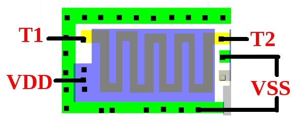
One common way to form resistors is to lay out one type of active area (ex: p) inside of another (ex: n) in a thin strip. Then reverse bias the junction to increase the resistance by shrinking the conductive area within the inner region. Example: (ST 24C02):
Which translates into:
I've grayed out the irrelevant parts and added labels for power and the two resistor terminals (T1/T2). The heavily doped green P+ areas form a connection to the P-well around the resistor while the resistor is N doped. VSS keeps a negative bias on the P doped region pulling charge away and thus making the region less conductive. VDD is applied to this essentially huge gate N channel transistor to keep it always on.
Diffused
Ion-implanted
Thin film
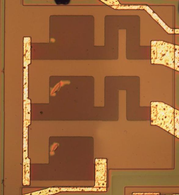
Thin film resistors “are fabricated by vacuum evaporation or sputtering of thin films of resistive materials directly on top of the oxide layer of the substrate” [Resistor Fabrication on Semiconductor Wafers]. Additionally, these can be laser trimmed by blasting away the metal. Example laser trimmed resistor (AD534):
Polysilicon
References
- Resistor Fabrication on Semiconductor Wafers: http://www.siliconfareast.com/resistor-fab.htm


