This is an old revision of the document!
Table of Contents
This page is very research orientated and information on it should not be trusted. TODO: this page should eventually have only compound logic gates, but is currently a sandbox for basic components. I'd like to substitute out these pictures for ones free of copyright issues to avoid any potential issues.
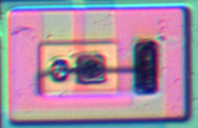
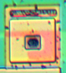
Transistor
Perspective:
Overhead:
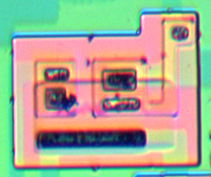
Real (transistor layer only, but top metal imprint can be seen in pink):
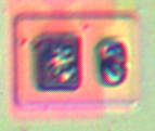
Diode
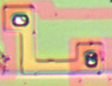
Resistor
Resistors seem to be grouped on islands with many other resistors. Resistance is a factor of the length of the trace, dopant, etc.
In MOS circuitry, resistors are avoided as much as possible as it is often much more cost effective to utilize transistors to form an equivalent circuit.
Capacitor
This component has an unknown appearance. Think it was difficult to form in early BJT circuits, so it is unlikely to be seen at all.
Logic gates
Buried layers
“You can also precede this by diffusing regions into the original wafer… Even though these regions are buried, it is still possible to align subsequent diffusions to them. When a diffused area is re-oxidized, a small amount of silicon is consumed (the Si in SiO2), thus creating a small depression in the surface.” (Designing Analog Chips)
References
- Encylopedia Britanica: http://media-2.web.britannica.com/eb-media/10/210-004-16A3DCFF.gif
- UC Berkeley EE 105 Microelectronics: inst.eecs.berkeley.edu/~ee105/fa06/lectures/F06-Lecture21-BJT.pdf
