
quiz:3h7e0f4_logic_data
Logic
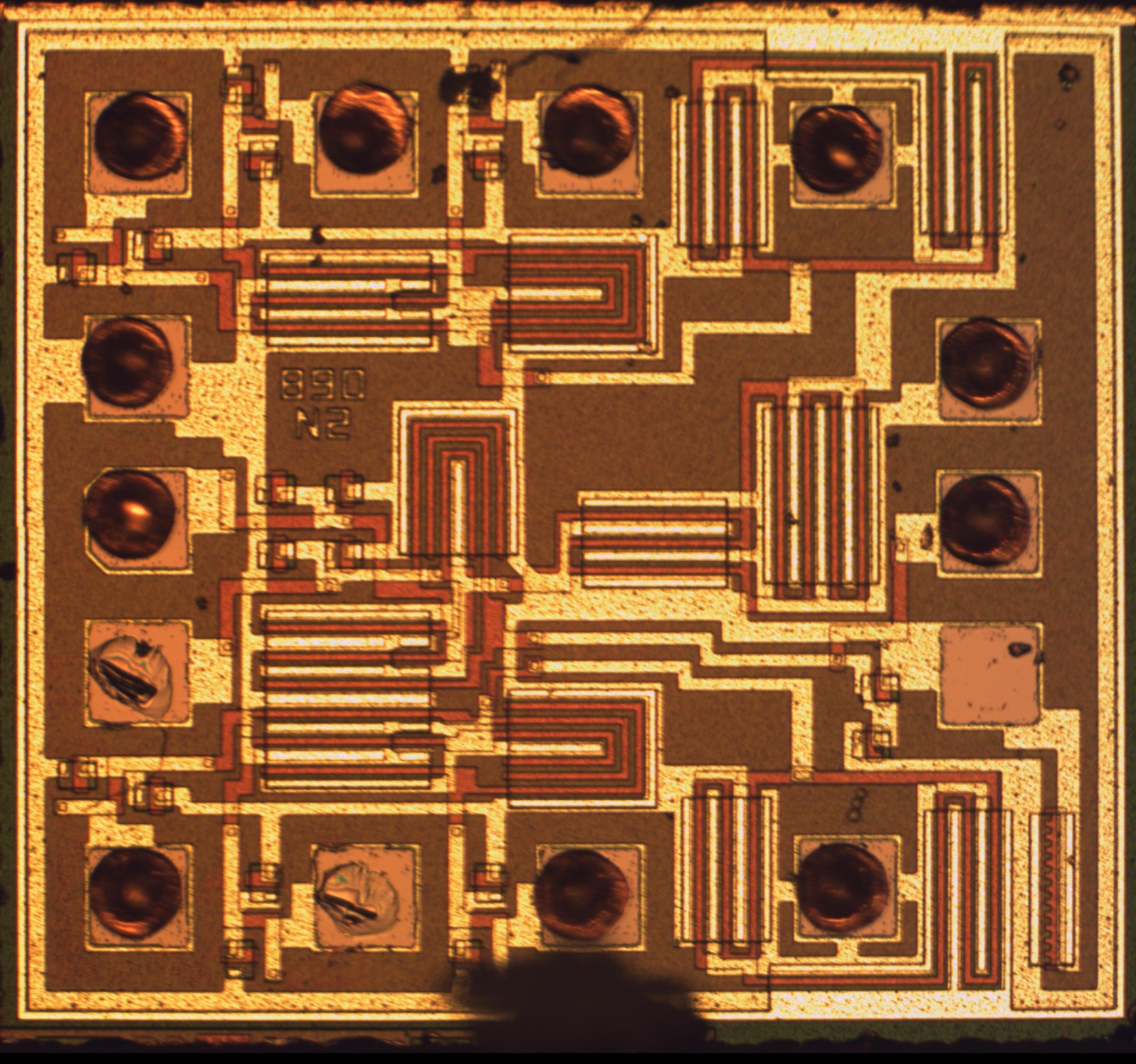
With the entire chip perimeter characterized we can start analyzing the logic.
- Basic logic chips are often regular with a few circuits repeated abeit in a very custom layout. How many instances of an isolated basic logic circuit are there?
- Detail
- The point of this is to figure out what the largest repeated circuit is. For example, if the chip was made of 2 flip flops we only need to analyze one of the two repeated circuits
- Exclude ESD protection
- Isolated meaning that you could form N truth tables because parts of circuits do not affect others
- Hint: think about input : output ratio and repeated layout
- 1
- 2
- 3
- 6
- 9
- [3]
- (1)
- Using our earlier analysis we have 9 inputs and 3 outputs. This should limit the maximum number of basic logic circuits to 3. We also see that there are three triple gates. Finally, if we look at the top section of the chip, only power and ground come down. Therefore, the top section of the chip is an isolated circuit.


- Now lets see whats connected to the output since its a little simpler than the input circuit. With an input of N1 (“net 1”) and output of O1 what logic function do you get?
- Detail
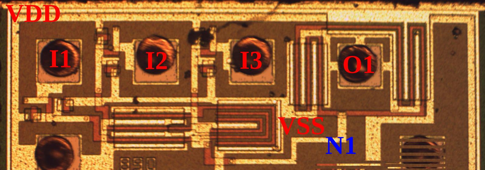
- Some of the other logic encroaching in has been shaded out
- Buffer
- Inverter
- Diode
- Or gate
- And gate
- [2]
- (1)
- The left transistor connects to VSS and the right to VDD. Each has three gates connected in several rings connected to the previous circuit by a contact from M2 to M1 a little above the label “N1”. VSS and O1 form interleaved fingers on the left to make an n channel MOSFET and VDD and O1 form interleaved fingers on the right for a p channel MOSFET.


- Time to run the gauntlet! Now you need to identity the final transistor circuit and the final question will ask you to piece everything together for the overall circuit function. What logic function is between I1, I2, I3 and N1?
- Detail
- Inverter
- 3 input and gate
- 3 input or gate
- 3 input nand gate
- 3 input nor gate
- [4]
- (1)
- The transistor on the left is p-mos since its connected to VDD and the right is n-mos since its connected to VSS. If all three inputs are given the right n-mos transistor will conduct and pull N1 low. If any inputs are low the left p-mos transistor will pull output high
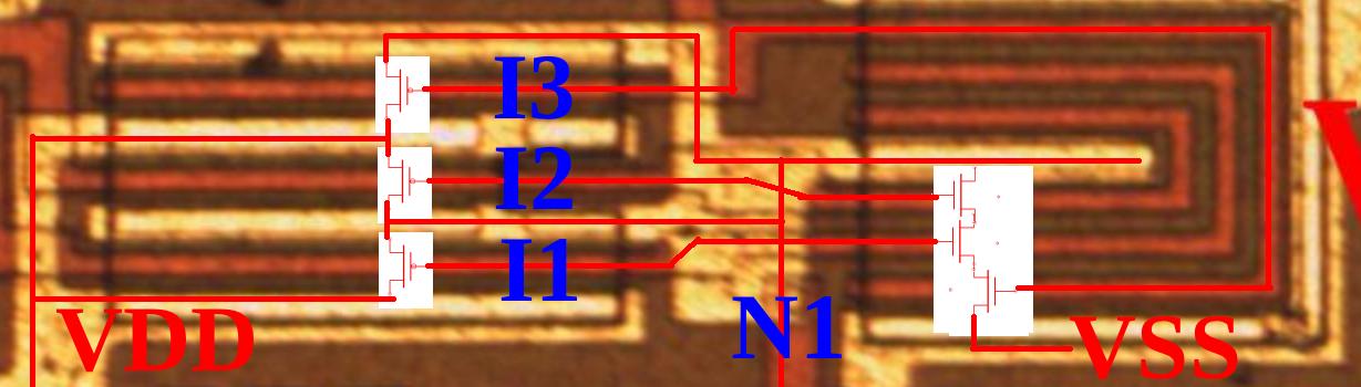
- This gives the following logic table
- ^ I1 ^ I2 ^ I3 ^ N1 ^
- ^ 0 ^ X ^ X ^ 1 ^
- ^ X ^ 0 ^ X ^ 1 ^
- ^ X ^ X ^ 0 ^ 1 ^
- ^ 1 ^ 1 ^ 1 ^ 0 ^
- This this is 3 input NAND as applying all three inputs to logic high turns the output off

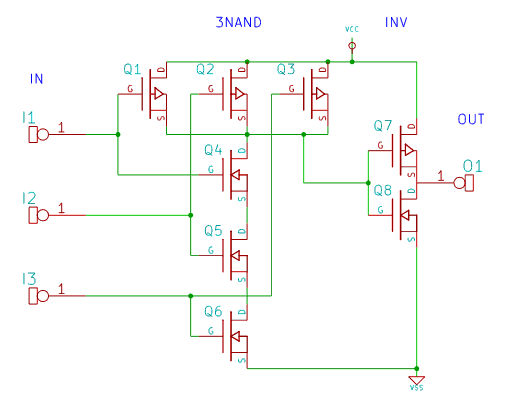
- Put it all together. What logic function does the overall chip represent? Combine the previous two logic functions feeding the output into N1 as the N1 input from the earlier question.
- Detail
- Above is a buffer w/ 3 copies on entire die
- Above is 3 input and gate w/ 3 copies on entire die
- Above is 3 input or gate w/ 3 copies on entire die
- Above is 3 input nand gate w/ 3 copies on entire die
- Above is 3 input nor gate w/ 3 copies on entire die
- [2]
- (1)
- The first circuit is a 3 input NAND gate fed into an inverter. Logically we have !(!(A + B + C)) ⇒ A + B + C or three input and gate. There are three of these circuits which I won't verify here but it should be pretty quick for you to verify for yourself if you understand the analysis. We're done!
- TODO: link to archive page with full chip info
- The chip is a Phillips HEF4073

quiz/3h7e0f4_logic_data.txt · Last modified: 2016/01/03 05:08 by mcmaster