Table of Contents
This page focuses on MOSFET technology. Pre-MOSFET is mostly only of historical interest
MOSFET theory 101
Pure silicon is a mediocre conductor but when its doped (either positive “p” or negative “n”) it becomes much more conductive. One simple application of this is to make a diode by placing n doped silicon next to p doped silicon. These charges cancel out and leave a poorly conducting charge neutral area in the middle. By applying positive voltage to the positive p side and negative voltage to the negative n side, the like charges repel and push the charge neutral area closer. As voltage is increased the neutral area shrinks and allows current to flow freely. Note that iss also possible to get current to flow in the other direction by applying a high voltage (avalanche effect) but this is not used in digital logic.
MOSFETs build on diodes by adding a control terminal to adjust charge between two similarly doped areas. For example, when positive voltage is applied to the gate of a N MOSFET it conducts. Similarly, when a negative voltage is applied to the gate of a P MOSFET it conducts. While real devices have many other critical details, this is generally sufficient detail to reverse engineer digital logic: while a logic designer has to make the system work reliably, a reverse engineer generally assumes the system works reliably.
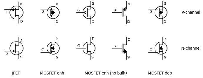
This (Wiki) image shows schematic symbols for different types of MOSFETs. When analyzing basic CMOS circuits only N MOSFETs (NFETs) and P MOSFETs (PFETs) are relevant. However, NMOS and PMOS also use depletion mode transistors. For most practical purposes, they can be inferred as resistors and the device physics can be ignored.
A note of caution: chip designers know this is how people think when they try to copy chips. They occasionally exploit real device physics even in digital logic to confuse reverse engineers (“traps”). For the meantime assume that circuits work as described above but be mindful that there are exceptions.
MOSFET layout 101
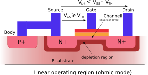
With some high level theory, lets now look at how real world MOSFETs are built. Above shows a typical cross section (derivative work). This is basically the theoretical discussion with the addition of a body terminal to isolate transistors from their neighbors.
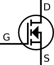
That transistor is represented by this schematic symbol (source). Recall that a diode is formed when a P and N region meet. And that's why the schematic symbol has a diode triangle: it represents the body diode. For most reverse engineering purposes this can be ignored.
There are many ways to make a real device. To illustrate, here is a gallery of different real transistor constructions.
Gate
In general, there are three types of FET technology (in chronological order):
- Early aluminum metal gate
- Polysilicon gate
- Metal gate w/ high-k dielectric
Within each of these, especially polysilicon gates, there are many variations.
Examples
Gate: poly
RSA SecurID 1C
Some of contact metal can be seen on the bottom but the gate itself is poly. The CMOS page details its use in an inverter
Xilinx XC2018
Similar process to the SecurID. Left middle has a via to poly. The poly extends right over an active area to form a transistor. The active area has contacts at top and bottom.
MOS 6522
Above: delayered showing poly (textured orange), active (orange), and buried contact (shadow)
The top polysilicon connects is driven by a via at top left. It crosses the active area to the right to form a transistor.
The bottom transistor side connects directly from active to poly via a buried contact. This poly goes off to bottom left to drive another transistor.
MOS 6526
Above: top metal image
Active area enters lower left and meets poly at a buried contact. The poly sweeps right to up to form a transistor separating the via from the active area at the right of the image.
CMOS quiz
See quiz for analysis
Gate: early metal
MOS MPS7083
Above top: top metal. Bottom: Al and some SiO2 removed w/ SiO2 thin film interference showing oxide thickness
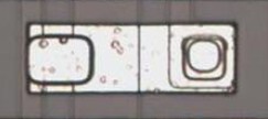
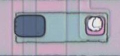
Typical metal gate CMOS transistor as used in non-trivial chips (ie CPU). The gate driver comes in on the right through an active area. The SiO2 has a cutout to allow placing a (Al?) via up to M1.
M1 goes left where it meets an active area. The teal SiO2 M1 area has thick oxide that prevents it from coupling to the Si below. However, the dark blue cutout brings it much closer (but not contacting, ie an “isolated gate” FET) such that its able to induce charge into the substrate below. Therefore, while metal crosses several active regions only one transistor is formed.
While the metal does spill over to some adjacent areas there are several things that prevent them from becoming an effective transistor:
- They do not fully cut off active areas
- These areas are likely biased such that adding additional charge wouldn't do anything
Fairchild CD4011
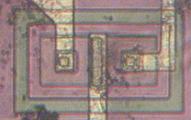
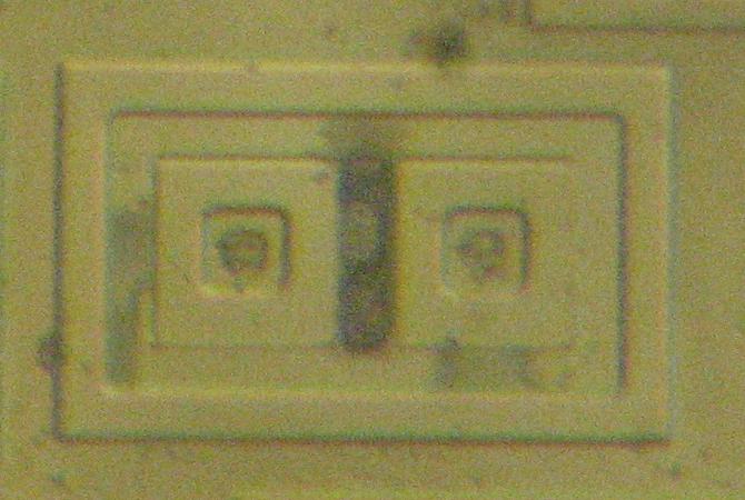
Above top: original transistor. Bottom: very siimlar delayered transistor
These textbook style metal gate transistors are rare in real devices. They are similar to the preceeding MOS transistor with cutouts for both the gate and vias. However, the doping is very different. The areas immediately to the left and right of the transistor must be opposite doping to the center and surrounging area (which apper to be doped the same per the delayer image). The via features are due to ohmic contact / windowing. I'm guessing the green layer is the opposite doping ie N if the center is P) and the layers on either side of it are the same doping based on thin film interference color. However, I'm still unclera why there are three different main regions.
Consider staining these to get more info.

