Table of Contents
Introduction
Mask ROM is used for high volume ICs that can sacrifice flexibility in changing the program for large volume production cost savings. Stand alone mask ROMs are also produced such as the MCM6570. These are most commonly found in videogame cartridges. These chips can be read directly, there is no need to use image processing to decode them. Note however that because such chips are easy to read they often are supplemented by security processors to prevent trivial cloning (ex: Nintendo's CIC series of chips).
Small ROMs are also used to form logic arrays such as for CPU microcode.
Logic familities
NOR
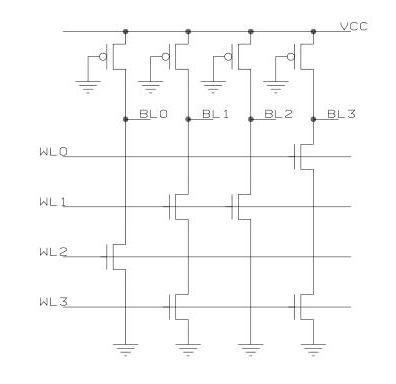
Above: NOR examples schematic. Copyright 2005 Sergei P. Skorobogatov, used with permission
NOR ROMs work by pulling up the bit line to VCC. When a word line is select some mechanism may be present to bring it low. Thus it is a “NOR” because output is a 1 unless any of the bit lines bring the output low. For example, say WL0 is 1 and the rest are 0. BL0 produces a 1 because nothing shorted it to ground but there is a pullup to VCC at the top. Similarly for BL2, both the WL1 and the WL3 transistors are off allowing to output a 1. However, BL3 outputs a 0 because the transistor at the intersection of WL0 and BL3 is on, shorting the output to 0.
OR
“There is an OR structure as well but the only difference between it and the NOR structure is that the transistors are connected to VCC instead of VSS” [Semi-invasive attacks, pg 28]
NAND
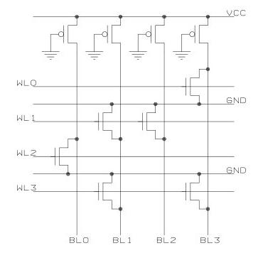
Above: NAND ROM reference schematic. Copyright 2005 Sergei P. Skorobogatov, used with permission
These are the logical complements of NOR ROMs. Instead bringing lines low through some sort of switches in parallel, the switches are in series. By selecting all switches not in the select row to turn on, the presence or absence of a switch in that region determines if the output changes state. For example, in above diagram output bit lines have a pullup transistor. Say WL1-3 are asserted but WL0 is not. BL0 will get a 0 because all transistors in that line were on (just the one at WL2) causing BL0 to short to ground. Similarly, BL1 also outputs a 0 because both the WL1 and the WL3 transistors are on to short out BL1. However, BL3 outputs a 1 because while the WL3 transistor is on, the WL0 transistor is not on.
Technology
There are several ways to implement the switches above. Typically these are done through manipulating mask layers but post fabrication techniques also exist (ex: laser ROM).
Active layer
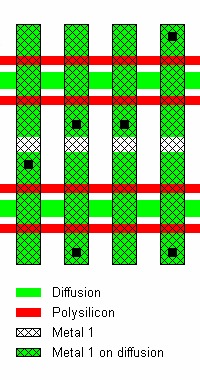
Above original caption: “Configuration and layout of MOS NOR ROM with active layer programming. This type of memory can be read optically.” Copyright 2005 Sergei P. Skorobogatov, used with permission
Contact layer
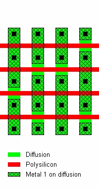
Above original caption: “Configuration and layout of MOS NOR ROM with contact layer programming. This type of memory can be read optically but usually requires deprocessing.” Copyright 2005 Sergei P. Skorobogatov, used with permission.
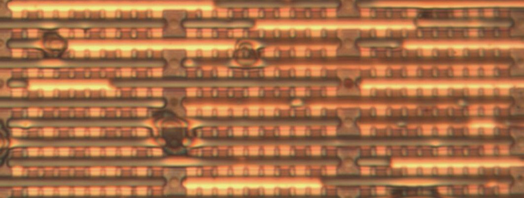
Typically requires delayering if a modern CMP process but older ROMs show the contacts through the metal. In the above image many transistors are formed but only a few are actually connected. The ones that are connected to the bit lines form the driving transistors that, if any are on, bring the output low.
Metal
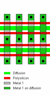
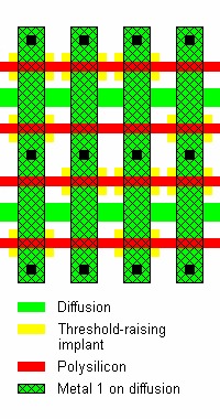
Above original caption: “Configuration and layout of MOS NAND ROM with metal layer programming. This type of memory can be read optically.” Copyright 2005 Sergei P. Skorobogatov, used with permission
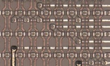
Easy to read optically. In above image transistors are formed everywhere. However, some of them are essentially bridged always on by putting metal over them. In theory I imagine that the contacts between several transistors shorted closed are unnecessary. For example, the top three contacts on the left. The middle contact essentially does nothing because both the surrounding transistors are bypassed.
Implanted
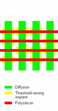
Above original caption: “Configuration and layout of MOS NOR ROM with programming using implants. This type of memory offers high level of security protection against optical reading.” Copyright 2005 Sergei P. Skorobogatov, used with permission
Above original caption: “Configuration and layout of MOS NAND ROM with programming using implants. This type of memory offers high level of security protection against optical reading.” Copyright 2005 Sergei P. Skorobogatov, used with permission
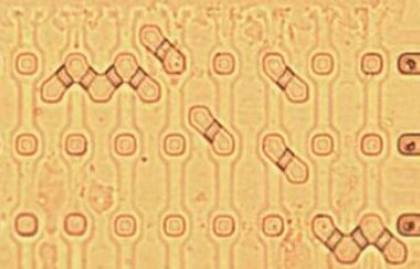
Implant ROMs essentially work by starting with a mask that has a grid of normal, working transistors. Then some of them undergo additional bombardment to change the voltage threshold. In the above examples the voltage threshold was raised such that the transistor is off regardless of the gate voltage applied. This is different than a depletion transistor where the transistor is normally on and turns off when biased.
Reading out
These can be tricky to read out, even on old chips, since they are not readily visible under a microscope.
Electronic
Try to find a test mode, glitch, etc by studying the die circuitry. Several chips such as the N64 CIC have been dumped this way.
Optical
Generally this level of doping is not visible to the naked eye. However, I've noticed that the implanted areas have sunken epitaxial areas that can be seen by oblique illumination. It may be possible to read an implanted mask ROM by exploiting this height difference by using oblique illumination, confocal microscope, etc.
Staining
This is the generally preferred method to read these out. See this page for information on staining with Dash etch. Other mixtures may also give results but this is the most industry standard.
Scanning capacitance microscopy (SCM)
AFM like technique that measures capacitance change by doping. This is believed to work for ROMs, although we currently don't have any solid data on this.
Scanning Microwave Impedance Microscopy
https://www.chipworks.com/about-chipworks/overview/blog/scanning-microwave-impedance-microscopy-smim
This is believed to work for ROMs, although we currently don't have any solid data on this.
Energy-dispersive X-ray spectroscopy (EDS)
Discussed this with someone and they think the dopants are too low concentration to be detected. It would be nice to get someone to actually do a scan and prove this.
Metal gate
TOOD: confirm this is how these work
Popular on older chips. Seems to always be NAND.
A CMOS transistor forms when a cutout is made to bring metal close to active area. Presumably these are otherwise like implanted depletion ROMs described above.
Examples
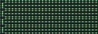
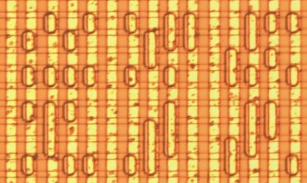
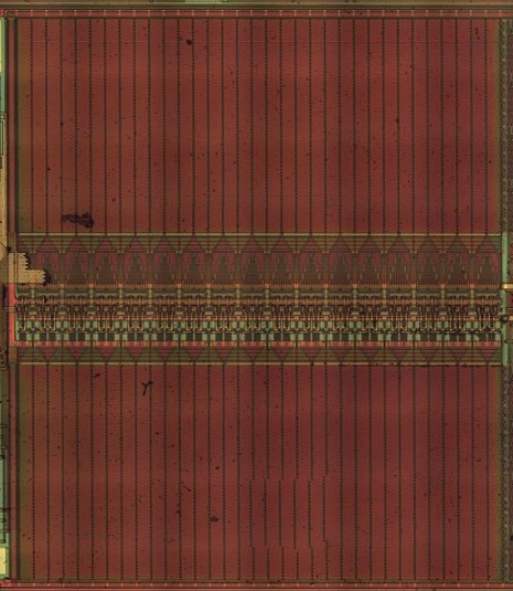
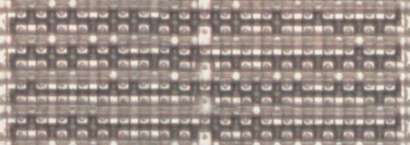
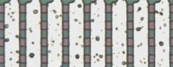
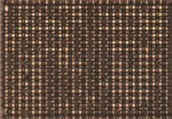
Nintendo 6102 NOR implant ROM
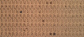
Motorola MCM6570 metal gate NAND ROM
TI TMS5200NL metal gate NAND ROM
Creative Technology CT1741 metal NAND ROM
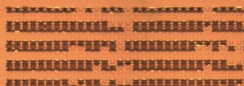
Motorola MC68010P8 active NOR ROM
RSA SecurID 1C vs 2C
Above: earlier 1C die
Above: later 2C die switched to implant ROM
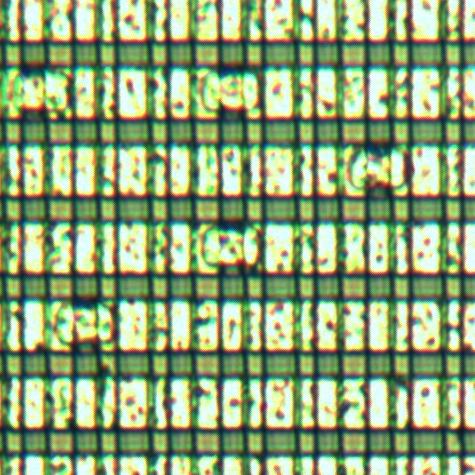
Above: 2C stained with dash etch to show bits
CBM 65CE02 active NOR ROM
Bandai Tamagotchi metal NOR ROM
HK HK628 active metal gate NAND ROM
Intel 80486DX
Decoding
I've created the SiliconAnalysis github group towards unifying misc tools into a recommended toolchain. At a high level flow looks like this:
- Use a tool to generate a spatially equivalent 2D array of 1's and 0's
- Use rompar as an individual
- Use djangoMonkeys to crowdsource
- Both of these tools can produce CV training data
- Feed into the zorrom library to decode into a binary
- Knows how to order bits
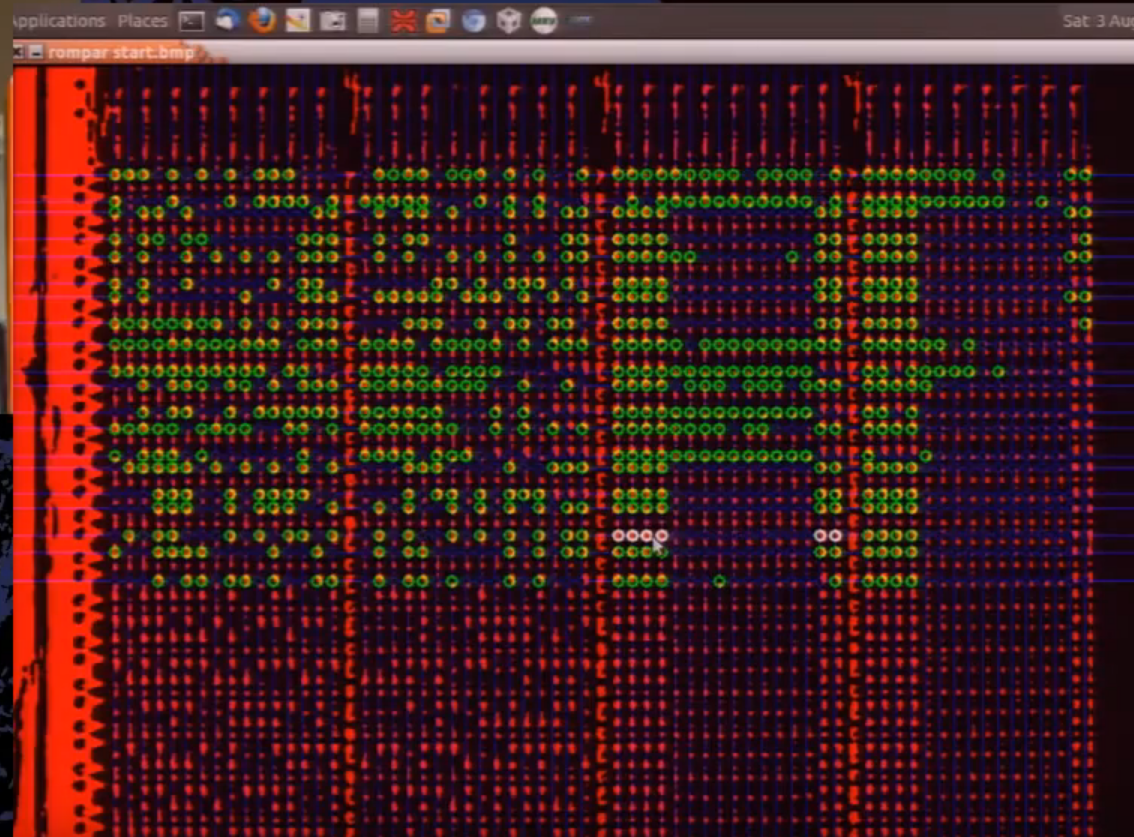
rompar by Adam Laurie
http://oamajormal.blogspot.co.uk/2013/01/fun-with-masked-roms.html
Code is not yet released at the time of this writing but looks to be a good tool to try out. Good article highlighting some of the problems optically reading mask ROMs and how they get around it.
djangoMonkeys
typingMonkeys
Original MAME mask ROM crowdsourcing project. Written in PHP, deprecated in favor of djangoMonkeys
Misc
Considerations for preparing SEM images for automatic decoding: http://recon.cx/2013/slides/Recon2013-Olivier Thomas-Hardware reverse engineering tools.pdf
Travis Goodspeed tried to have a contest to decode some automatically and unfortunately got no submissions. The MCM6570 had two different type cell sizes (only one shown above), although I get the impression this is unusual. Ideas:
- Generic feature recognition
- Horizontal projection profile, possibly using color differences. Very sensitive to angle though, so might not be practical
- Signal based: above design has additional images on top of base. Filter out signals from repeating pattern and analyse remainder
Tool1
An unnamed tool. I (mcmaster) have a copy of it but was requested not to post binaries and/or screenshots. However, some general feedback:
- Their tool works by thresholding with misc tools to help see this
- Bits are selected by drawing a box on the center of where the bits go. Then you tell it how many in rows/cols
- Has pan and zoom, which made it much easier to use than rompar for the large dataset I was working with
- Author says that in their experience bits are always on the same grid pitch, even if there are gaps
- Distributed as Windows executable
References
- “Semi-invasive attacks - A new approach to hardware security analysis.” Sergei P. Skorobogatov.
- “Image decode Project”: http://www.progettoemma.net/dump/

