
quiz:3h7e0f4_pinout_data
This is an old revision of the document!
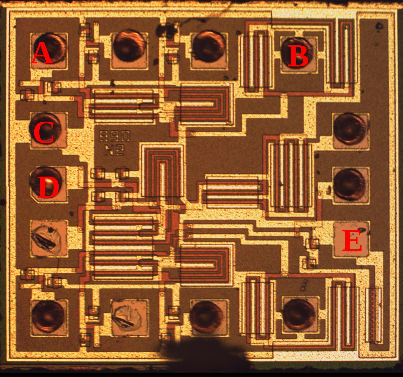
Pinout
This module steps you through finding the basic pinout of the device before starting to really dive into the logic.
- Identity pin 1
- Detail
- Pin A
- Pin B
- Pin C
- Pin D
- Pin E
- [4]
- (1)
- Many chips make pad 1 irregular or put an indicator marking on it. On this chip it is a pentagon. Some even go so far as to actually number every pin, although that is less common. If there wasn't something like this on the die or verification is needed one can of course also prepare the chip live (or at least with pins in place) by not doing bare die decapsulation.


- Identity VDD
- Detail
- Delayering showed this to be a 2 metal chip with no poly (hint: CD4000 series metal gate)
- Hint: you need the padframe and some knowledge of CD4000 to make this easy
- Pin A
- Pin B
- Pin C
- Pin D
- Pin E
- [3]
- (1)
- You should be able to narrow it to pin C or E without too much trouble as they are the only ones that spider out all over the chip. Metal gate chips are exceedingly rare and usually only show up as CD4000. Combined with this being a very simple chip it makes it a good bet. Assuming that, most CD4000 chips put VDD as the highest numbered pin and VSS as the pin opposite. In our chip we have power pins at pin 7 and 14 which matches this. Therefore, pin 14 is VDD.

quiz/3h7e0f4_pinout_data.1451794781.txt.gz · Last modified: 2016/01/03 04:19 by mcmaster