Table of Contents
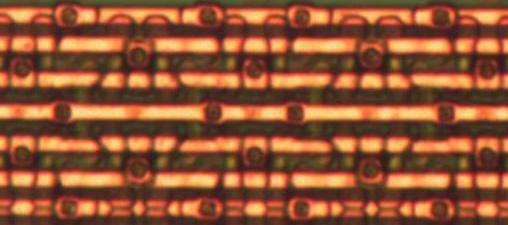
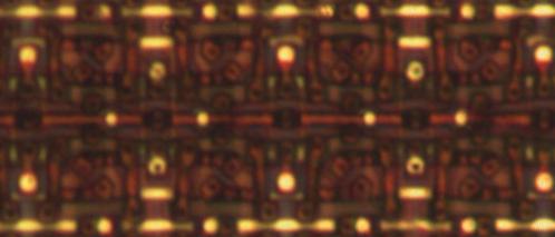
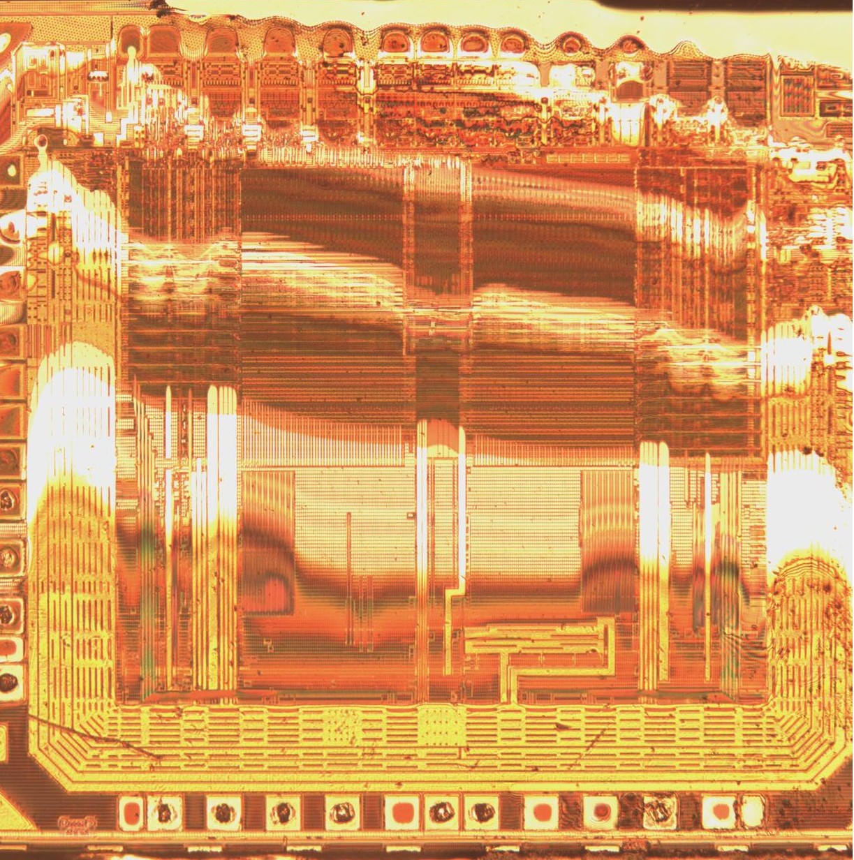
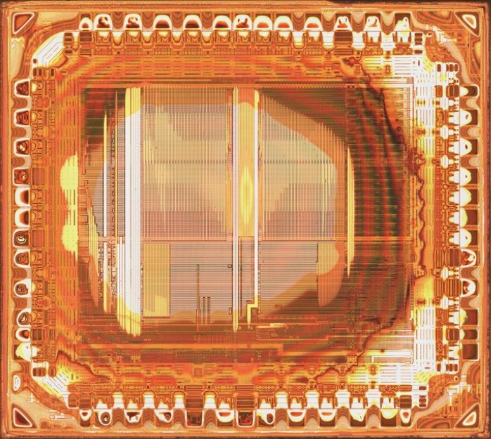
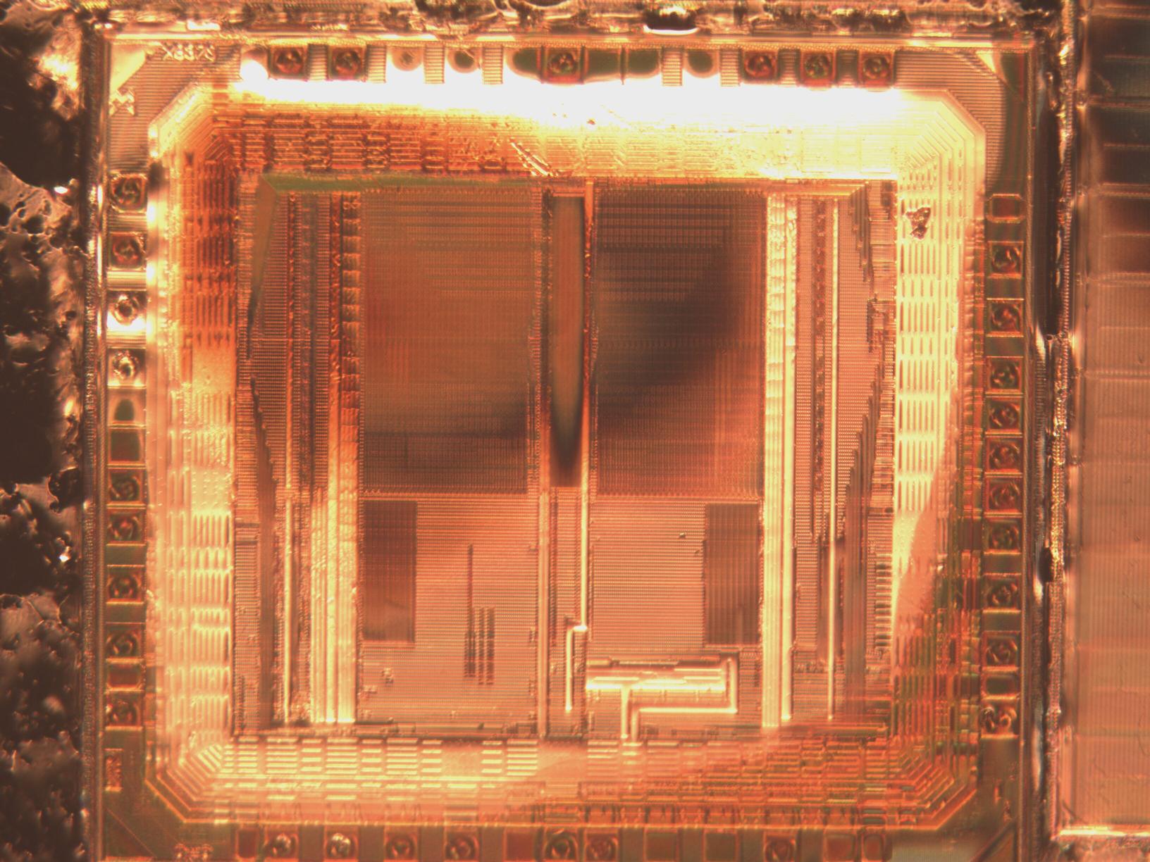
Above: a non-planarized chip before and after lapping
Lapping is more or less the process of using an abrasive on a plate to slowly remove material from a sample. This makes it distinct from polishing in that while polishing also produces smooth surfaces they don't maintain uniform flatness across the entire workpiece. However, the distinctions blur and are often used interchangeably both on this page and in literature.
Within integrated circuit analysis two types of lapping are often employed:
- Parallel polishing: used to remove one layer at a time from the top of the IC or for final backthinning
- Sectioning: used to smooth an IC that has been precisely cut in half to view the layers
The focus of this article is on parallel polishing and any techniques will refer to that unless otherwise specified. This same process is used to manufacture ICs in a process known as Chemical Mechanical Polishing (CMP). This is a key part of wafer polishing and copper damascene. Furthermore, this focusing on automatic polishing, that is using a machine, rather than manual techinques as they are more repeatable.
Quick overview of typical process: a sample is wax mounted to a stainless steel fixture. The fixture is then put on a spinning disc that is sprayed with a colloidal silica slurry. The sample is occasionally inspected for completion, possibly aided by a micrometer or mechanical setpoint on the polishing fixture.
General advantages:
- On planarized chips, can reveal a layer at a time
- Less expensive than RIE
- Avoids HF and other nasty chemicals used in RIE
Disadvantages
- More expensive than wet chemical etching
- More setup time than wet chemical etching
- Messy
- IC must be reasonably clean
- May not work well on non-planarized chips
- Slow: one layer can take hours, days even
[Allied Tech parallel lapping] reccomendations:
- 1 drop every 2 seconds
- More drops ⇒ more abrasive ⇒ faster
- 205 to 225 RPM optimal
- Do not rotate the specimen at its center or you'll get rings (“donuts”)
- “Rotation is key when trying to evenly polish a sample. It allows the sample to be polished from all sides, eliminating smearing and maintaining flatness.”
- Markers on lapping jigs are for reference only, do not use them alone to place sample
- Monitor material removal based on time, using experience as a guide
- Dial indicators are not recommended to monitor lapping progress due to uncertainty in cloth compression
- More pressure ⇒ faster but less even (sample corner rounding)
- Wet platen with water instead of colloidal silica
- Their system uses a separatory funnel w/ stopcock instead of slurry pump
- Uses polishing cloths
- “Different cloths are used for either copper or aluminum metal circuitry”
- Uses adjustable height instead of weights or pneumatic
- “If it does not make sufficient contact, it can take days to remove a single layer”
- Instructs simply letting the die settle on the fixture while was is hot, is not pressed against hard surface
- Maybe should try…means that any imperfect but consistent polishing will be repeated
- Alternatively just double stick tape it on
- May go through cloths as often as two per sample
Machine
Facing off
Before a fixture is used it should be faced off to ensure that the surface is parallel
For tripod fixtures:
- Scribble on the fixture with a Sharpie
- Lap for a few minutes (or less if everything comes off quickly)
- Observe what area is removed
- Adjust tripod system to favor the areas that were not removed
- Repeat until desired parallelism is achieved
This procedure can also be used to verify that a sample is set reasonaby well by scribbling on it and doing a short polishing cycle
For other fixtures:
- Lap until surface is smooth
If the surface has damage you may consider using fine grit sandpaper first
Pads
Poromeric example
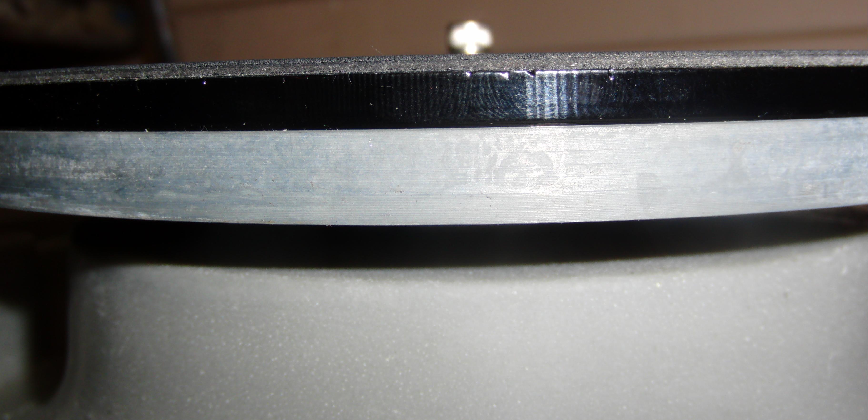
Above: typical stackup seen on JM machine consisting of (top to bottom):
- MTI 8“ Poromeric Polishing Pad (PSA) for final polishing - EQ-PP-8PSA-PC
- 8” Mater Plate ( Backing Plate ) for PSA Diamond plate, Sand Paper & Polishing Pad - EQ-MBP-8-2
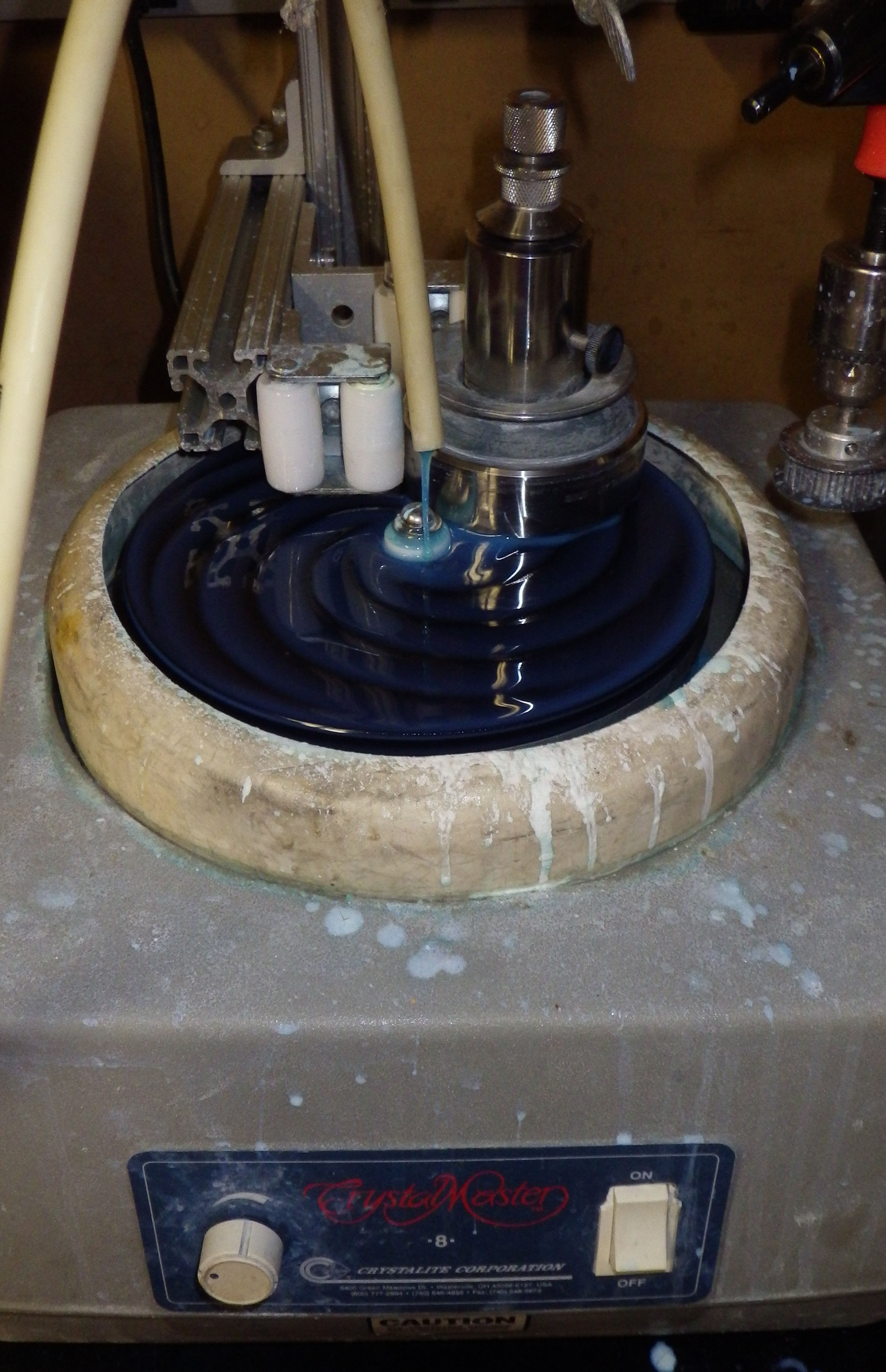
- CrystalMaster 8 master lap (aluminum platen)
The first, the poromeric pad is the most important. It is essentially a soft pad to move abrasive around without actually scratching the die. The next forms a smooth surface on which the poromeric pad rests. Finally, the master lap is the interface to the machine itself and has ridges to keep backing plate in plate.
Originally the machine had a steel backed diamond pad directly on the master lap (attached with adhesive, removed with acetone + heatgun). In this setup the steel backing is much stiffer than the polishing pad and so serves as the backing plate.
Non-PSA
Asked TedPella about how to use non-PSA pads:
Q: Re: Non-PSA lapping films
How are these intended to be attached?
I noticed they are lower cost but I don't understand how one would use them.
Can you point to an example workflow/setup using them?

A:
Some polishers have a ring that fits on the disc and holds the  lapping film in place.
You can also try applying  a thin film of water on the disc under the film.
If moderate polishing pressure is used this method  is satisfactory.
For  more aggressive polishing, a spray adhesive can be sprayed on the disc.

The easiest  solution is to use PSA backed film.
Abrasive (slurry)
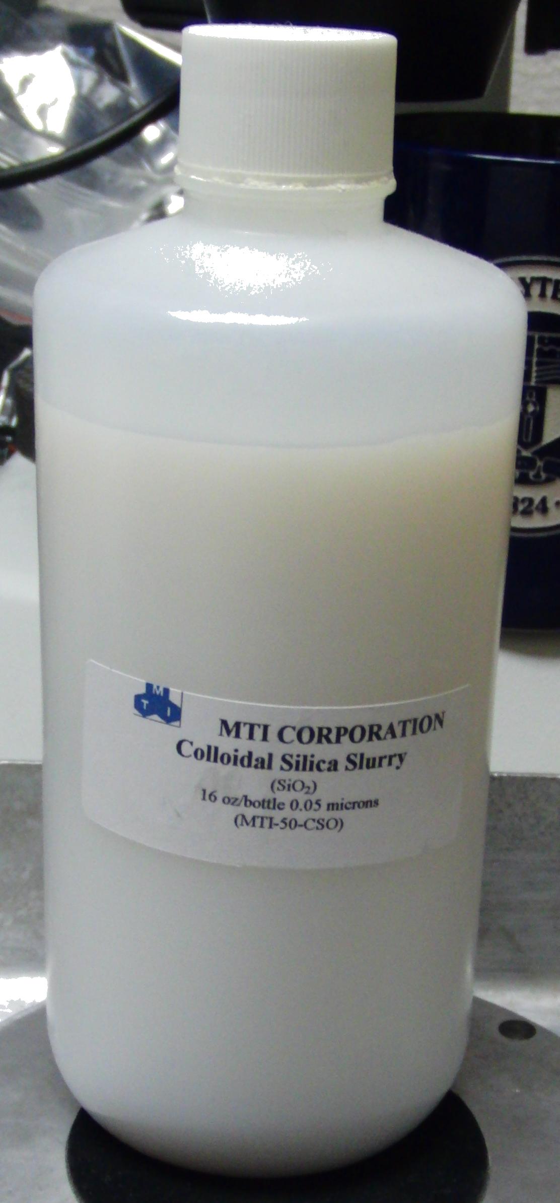
Most common is colloidal silica, a suspension of SiO2 in water. Comes in a variety of particle sizes. I (JM) use 0.05 um for everything so that I don't have to clean machine between runs and/or have two machines.
Originally I used MTI “Colloidal Silica (SiO2) Slurry for CMP, 16 Oz/ bottle at 0.05 micron - EQ-MTI-50-CSO” but now am using Ultratec 2397.1 (Blue Non-crystallizing 0.05 um Colloidal Silica) because I can get it in larger size / costs less than half per volume of the MTI at that size.
Ultratec offers solutions in different colors presumably so that you can easily tell 0.03 um solution from 0.05 solution.
Colloidal Silica mixed with Alumina Suspension
To be tested
A buehler representative advised to use a mix 50% Colloidal Silica + 50% Alumina suspension when lapping wafer and die.
Product link: http://www.buehler.co.uk/produits/consommables/polissage-a-loxyde.html
Sample mounting
Adhesive
Sample is pressed into it with hot wax on a hotplate [Parallel Lapping of Devices for Deprocessing, Allied Tech parallel lapping] or super glue. There are ridges in the sample holder to help the wax stick. I use “821-3 CrystalbondTM 509 Clear” which seems to work pretty good. I tried a few alternatives like superglue but didn't get very good results (dried too quickly and didn't hold very well). With wax, working time is much longer and holds much better. The heating/cooling cycle does add a little extra time but not too much. It also allows reworking by re-heating the wax if it doesn't set right.
I played a lot with wax thickness. Certainly shouldn't be nearly as thick as the dies but still playing with whats ideal. Thin wax layers (like above) are easy to work with to move the die around without significant wax pooling. However, I've found that slightly thicker wax layers can be advantagous to force a little wax on sacrificial die (see below) edges to help them stick together. This keeps it more planar during pressing and helps prevents dies from separating as the wax is squished.
Maintaining planarity
Above: a non-planar die. The top was higher and thus had more pressure on it and was lapped first
Causes:
- Contamination: debris above or below die tilted it
- Damaged sample
- Poorly manufactured sample (probably won't get shipped if its noticibly bad)
Rounding
Above: a die with rounding. Although its planar its worn a lot more around the edges
There are two issues sacrificial dies can correct:
- Excessive edge wear: presumably this is a boundry condition where the pad is compressing, adding additional force, as it enters the cycle
- Non-planar mounting
[Allied Tech parallel lapping] suggests to leave at least 2 mm on each side to prevent rounding. If its something you manufactureed, scribe it as such. However, a RE rarely has that advantage. Instead, place sacrificial dies next to die to decrease rounding (as opposed to far away to increase planarity).
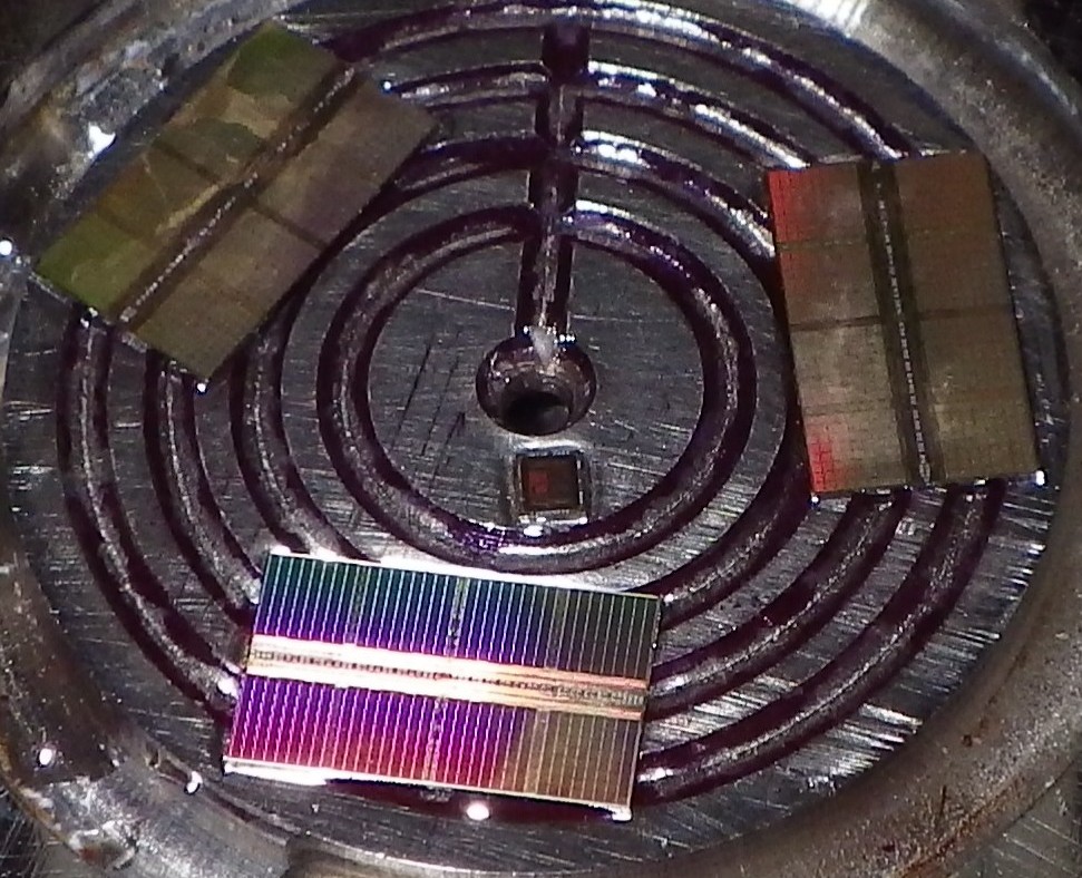
If possible add some blank dies to increase the effective plane size. Use at least three to form a plane, more should be fine. They must be the same thickness and placed evenly apart so that the fixture spins evenly. Probably needs to be within a few um and closer is better. 20 um has been shown to have no effect at all.
Sacrificial dies must be matched very closely in height to the sample. 20 um differences have been observed to have significnat impact (bear in mind a layer is only 1 um). I ordered a high resolution micrometer to help with this (Mitutoyo Digimatic Micrometer 293-761-30). Make sure to clean them well to ensure a good measurement. For actual setting I don't think they have ot be perfectly clean as the wax on both sides should help to even out any small imperfections.
Additionally, if a die is mounted on center it will form rings where the wear is strongest. To fix this mount the die away from the fixture's center of rotation. In my fixture its difficult to mount the die at the center so I haven't run into this problem
Balancing
In my fixture the carbide fixture pads provide more resistance than the sacrificial dies and so the sizes don't have to be matched very closely. If you mount a large sample you should consider balancing it to keep the spin force even.
Reworking
If wax gets on top of the dies, I do the following:
- Let the jig cool down
- Very lightly soak a Kimwipe in acetone and hold with metal tweezers
- Put airflow over jig
- Evaporates acetone runoff quickly so that it doesn't pool and dissolve substrate wax
- Gently wipe top of die with damp Kimwipe
- Repeat wiping until surface is clean
JM mounting procedure 02/05/2014
Equipment:
- South Bay Technology lapping jig
- Flat hard surface (steel plate)
- Stainless steel weights
Consumables:
- Crystalbond 509
- Sacrificial dies
Prepare sacrificial dies:
- Optional: cut die on hard surface using hobby knife. It should split cleanly
- Clean die in ultrasonic bath
- Ultrasound should break off any weak areas
- Consider cleaning in dedicated container: will shake off a lot of debris
- I always do acetone, suds, and then IPA in 1 minute or less rounds
- Lay dies in clean container for easy pickup
Prepare wax:
- Place wax cylinder in ziplock bag
- Gently hit wax cylinder with hammer to break it up into large pieces
- Roll large pieces with metal cylinder to break it into powder
Prepare press weight (round):
- Tear off piece of wax paper
- Place wax paper over dead weight
- Crumple wax paper edges flush against sides of dead weight
- Zip tie wax paper to dead weight
- Side zip ties down to re-tension if it comes loose
- Zip ties can be reused
Steps:
- Heat hot plate to melting point of wax
- If unknown: put some wax on jig and slowly turn up heat until it melts
- Remove sample holder from jig
- Place sample holder on hot plate with sample side face up
- Sprinkle wax onto sample holder
- Let wax melt
- Roll out wax flat with a cold (room temp) 1“ stainless round
- If necessary: add additional wax and re-roll until flat
- If necessary: wipe up any excess wipe that is beyond the sample area
- Generally does not matter
- If applicable: clean out center of jig by briefly turning cold drill bit in center
- My jig has a hole in the center
- Wax can flow into hole and prevent ramrod from screwing into jig
- Pickup sample holder with pipe wrench (hot!) and place on work area
- I find it useful to work under inspection socpe
- I put a thin teflon sheet down to insulate it
- Place sample die near but off center of jig using tweezers
- Place 4 adjacent sacrificial dies using tweezers
- May require a bit of force to get them to stick instead of push apart
- If wax squishes up, see cleaning procedure
- If space permits: place 3+ planar sacrificial dies in triangle pattern using metal tweezers
- Pickup sample holder with pipe wrench (hot!) and place back on hot plate
- Let sit for a minute or so until hot again
- Pickup sample holder with pipe wrench (hot!) and place face up on steel plate with a teflon sheet on it
- Steel plate by itself will cool sample holder rapidly. Teflon sheet keeps it hot longer for better settling
- Place press weight (wax paper facing down towards the dies) on top of dies to planarize them
- Do not move once placed: wax will immediately stick to it and cause a huge mess
- If you need to re-do let it cool, clean dies, and then re-heat/replace
- If you felt it rock or similar, you have poor placement and will get bad results. Verify it was centered and verify die thicknesses match
- Let wax cool (3 minutes)
- Reccomendation is 20-30 but I haven't seen any evidence you need to wait that long
- Slide zip ties off of press weight
- Remove press weight, keeping wax paper in place (should be stuck to dies)
- Peel wax paper off of dies. It should come off easily
- Verify even coat of wax is on target and sacrificial dies
- Verify adjacent sacrificial dies did not noticbly separate during press
- Repeat until dies are clean
- Soak kimwipe in IPA
- Rub sample holder into kimwipe, dies facing towards kimwipe
- NOTE: if something does not come off, it may be Crystalbond and not wax paper. Consider re-setting although it can be cleaned off using the rework procedure
- Attach sample holder to jig
Notes:
- If necessary (especially with small samples), remove jig from hotplate and put under microscope when placing. The jig cools slowly and you should have plenty of time
- You really should use steel tweezers. Carbon fiber or plastic tweezers melt easily and cause the die to stick (way before they visibly melt), leading to poor placement
- Clean tweezers any time they get contaminated to prevent dies from sticking
JM unmounting procedure 12/26/2013
After you are done lapping the fixture needs to be prepped for another run. In order from longest time / safest to quickest / most aggressive
Steps when sample must be recovered (patient method, use for important samples):
- Remove sample holder from fixture
- Clean sample holder with water
- Clean sample holder with acetone until bulk wax is gone
- Change acetone bath
- Let sit for a few hours and/or overnight to let soak under dies
- Elevated temperature should help but haven't tried
- Gently remove sample with carbon fiber tweezers. If its not loose let soak longer
Steps when sample must be recovered (fast method, typically used):
- Remove sample holder from fixture
- Clean sample holder with water
- Clean sample holder with acetone until bulk wax is gone
- Use heatgun to heat up dummy dies and remove by pushing them off with a teflon scrap
- With the surrounding wax gone they should come off easily once they can slide
- Wipe up any excess wax
- Let cool
- Attach sample holder to fixture for storage
Steps when recovering sample is less critical (reuses wax, use for throwaway samples):
- Remove sample holder from fixture
- Clean sample holder with water
- Use heatgun to heat up dies and remove by pushing them off with a teflon scrap
- Wipe up any excess wax
- Let cool
- Attach sample holder to fixture for storage
After sample removal:
- Soak in acetone until all visible wax is gone from sample
- Clean in fresh acetone to remove residue
Tips:
- Use low air flow on heatgun to avoid blowing dies away
- Use a hotplate if you have problems. It will take longer but is more controlled
- Do not re-use dummy dies
Automatic lapping procedure 02/05/2014
Above: typical top metal planarity on a *small* (< 2mmx2mm) die. Larger dies give much better results and also tends to get better as more layers are removed
Steps:
- Mount sample using wax procedure on this page
- Prepare polishing pad
- Spray pad with water
- Start machine: spin it up gently to get an even coat and knock off debris
- Turn on slurry pump to try to get 1 drop per second or two
- Position slurry spray to center of pad so that it diffuses evenly
- Stop machine
- Place lapping jig without sample holder to condition pad a little
- Start machine, let run at low RPM for a few minutes
- Run sample
- Attach sample holder to jig
- Set jig 125 um off of surface
- Stop machine
- Quickly but carefully place jig onto pad
- Start machine
- Adjust machine to run at around 300 RPM
- Run for desired length of time
- Requires experience: many factors (die area, process technology, speed, jig weight etc)
- Start out conservative (say a few minutes)
- 10 minutes tends to work well for most chips I do
- Stop machine and remove sample holder from jig
- Place sample holder in water
- Place jig back on lapping machine (without sample holder)
- Start machine and let run at low RPM
- Conditions pads / stops it from drying out
- Do not touch the slurry controls
- Examine sample to determine if it needs additional time
- Generaly rough progress can be gauged with naked eye
- Use microscope when more detailed inspection is required
- Repeat until done
Cleanup:
- Spray water onto pad to keep it from drying out
- Run slurry pump in reverse for a few minutes to drain feed
- Squirt water into feed to flush out anything near end that could dry out
- Fully submerse jig in water to clean it
- Turn on machine and spray additional water on pad to do a token clean
- Sometimes I run my finger on the pad to squick out additional slurry
- Turn off machine
- Unmount die from sample holder
Misc:
- Keep machine stoppage to a minmum. CMP solution dries quickly and can form damaging crystals
- Flow rate should be low, say 1 drop every second or two. Pad should be damp, not wet
- Causes severe rounding from more abrasive at edges than in center of die
- Prefer higher speeds, say 200-300 RPM
- Add sacrificial dies to reduce pressure as needed
- Die thickness varies lot to lot. Check them carefully
- Cleaning wax paper off
- Soak Kim wipe in IPA
- Rub fixture w/ die against the Kim wipe until clean
- After setting dies, put back on hot plae before pressing
- More regularity in wax temperature when pressing
- Try to let dies stick together, cleaning wax that made it to the surface if necessary
- Small bits of wax shouldn't matter since wax paper will absorb it
- Must thoroughly clean all wax off before lapping or it will add significnat masking defects
- Larger dies tend to be easier to work with than smaller
- Planarity tends to improve on lower layers. I suspect this is related to top layer not being planarized
- I tried to user higher slurry pump rate but soaking edge of pad to control how much made it up. I think this caused a severe slurry gradient, not reccomended
Wafer thickness
It can be important to put in dummy dies to get a nice parallel surface. Useful to know standard wafer thicknesses to purchase blank wafers.
General guidelines:
- 0.29 mm: DDR-1
- 0.44 mm: SODIM
NOTE: many dies are thinned. See table below for examples of approximate actual die thicknesses
From Wikipedia
| Diameter (mm) | Thickness (µm) |
|---|---|
| 25 | N/A |
| 51 | N/A |
| 76 | 275 |
| 100 | 375 |
| 125/130 | 525 |
| 150 | 625 |
| 200 | 675 |
| 300 | 725 |
| 450 | 925 |
But how to measure? You can of course very gently measure using dial caliper or micrometer. Alternatively take pre-measured dies and visually inspect to see which its closest to.
Example die thicknesses from JM inventory:
| Vendor | Die | Thickness (mm) |
|---|---|---|
| Xilinx | XC2C32A | 0.32 |
| Elpida | dd2516akta | 0.28 |
| Fairchild | 74f161a | 0.36 |
| hm5216805tt10 | 0.32 | |
| hy57v658020b | 0.32 | |
| hyb39s64800ct-8 | 0.38 | |
| Harris | 80C86 | 0.48 |
| htl | ht33s328256k | 0.27 |
| mt46v16m8 | 0.31 | |
| mt 48 lc16ma2 | 0.29 | |
| mt 48lc 16m8a2 tg-75 | 0.30 | |
| mt 48 lc2m8a1 tg-8b | 0.31 | |
| oki | m56vi6800d-10 | 0.28 |
| phillips | hef4052bt | 0.38 |
| siemens | hyb39s16 | 0.38 |
| samsung | k4h560838c | 0.36 |
| sst | mpf 39vf010 | 0.66 |
| ti | 68f483k e4 | 0.26 |
| vg264265bj | 0.43 |
This is mostly dies I have a bunch of such that they'd be candidates as blanks during lapping. This biases it mostly towards chips I scrapped out of RAM
Sectioning (for TEM)
Process analysis cuts dies at right angles. These are typically small stainless clamps that hold the die against the wheel with precise angle adjustment.
With wet etching
Flylogic uses both it and wet etching. As lapping through the SiO2 can take a while this significantly reduces processing time. They also use the finger method leading to non-planar laps. However, as they are only looking at specific chip areas this is acceptable as it tends to be flat enough over the area of interest.
My guess is that wet etching away the overglass could help reduce some lapping defects and could prove effective in combination with some lapping fixtures
Troubleshooting
[Allied Tech parallel lapping] general reccomendations if not polishing evenly:
- Not mounted correctly in fixture
- Debris between die and fixture (ie its not flat against it)
- Machine not calibrated
- Your IC sucks
Under/overworn areas
Suggestions:
- Clean your sample better
- Non-CMP or or other manufacturing artifacts
- [Allied Tech parallel lapping] suggests phasing speed to arm position since wheel spins faster further out than closer in
Tilt
Suggestions:
- Die is likely not flat
- Check for debris that prevented it from setting correctly
- Add more sacrificial dies to increase plane size
- Verify all sacrificial dies are the same height
- Verify die is securely held in place. Clean it better if not adhering to wax
Rounding
Suggestions:
- Apply less pressure (could include adding larger sacrificial dies to increase area)
- Add sacrificial dies
- Use less slurry. Pad should be damp, not wet
- Verify die is mounted off center
Manual
Without using a machine or jig, its possible to simply rub a die against a pad soaked in CMP solution. I did this before I got a machine and it worked to get some basic polishing results but is very labor intensive.
Slightly a step up is to use a machine without a jig. Some notes: tutorial
mcmaster notes
900 g Al round block
- P180 / 80 um used SiC: 140 mm3 / sec @ speed 3
- 460 - 423 = 37 um / min
- 5.3 x 11.0 mm = 58.3 mm2
- 37 * 4 * 58.3 = 8628.4 mm3 / min
- One die fractured after just one minute
- Probably too aggressive to use in practice
- 30 um new AO: 6.2 mm3 / sec @ speed 3
- Same area as above
- 1.6 um / min
- 1.6 * 4 * 58.3 = 373 mm3 / min
Removing pads
- 300 F optimal
- By 350F glue is too soft to come off in one piece
References
- Parallel Lapping of Devices for Deprocessing: http://www.southbaytech.com/appnotes/57 Parallel Lapping of Devices for Deprocessing.pdf
- Beck's failure analysis chapter “The Surface-Parallel Planar Microsection” (page 139)
- Allied Tech parallel lapping: http://jiam.utk.edu/new/PDF/Allied-Parallel-Lapping-Integrated-Circuits.pdf
- Allied Tech backside thinning: http://jiam.utk.edu/new/PDF/Allied-Backside-Thinning.pdf
- Cabot Microelectronics “Professor polish” series
-
- Single Die 'Hands-Free' Layer-by-Layer Mechanical Deprocessing for Failure Analysis or Reverse Engineering
- Tony Moor, with support from Gatan (Eli Malyanker, Efrat Raz-Moyal)
- Talks about sacrificial dies and other issues
- Professional equipment

