This is an old revision of the document!
Table of Contents
Passivation
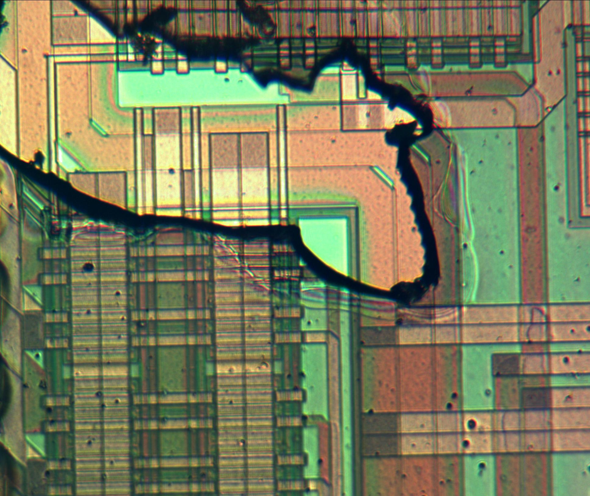
Protects the underlying circuits. Seems to be omitted on rare occasions or more likely at least something that decapsulation chemicals attack. When still on the chip it gives a cloudy feeling and should be removed for best results. Example of damaged passivation showing difference in image quality:
When the passivation is in good condition it can be difficult to discern if its still present. Also called overglass since its often made of SiO2.
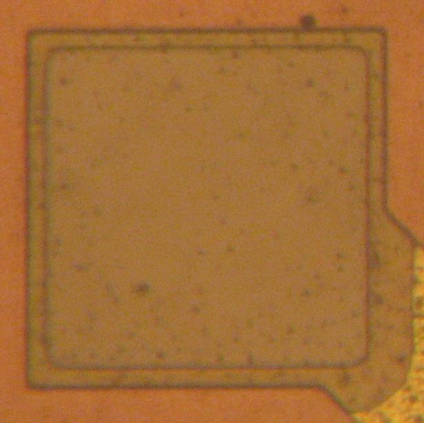
Pads
See main article
Straining
Tensile stress enhances electron mobility and compressive stress enhances hole mobility. [Kaeslin] Can be incorporated with the following:
- Package
- Adding Ge to Si
- Adjacent layers with different lattice spacings
- Intel Core Duo: SiN cap for tensile stress, epitaxial SiGe for compressive stress
- In particular, this might show up on the die
Does not seem that this is common and is only seen in very high performance ICs.
Test structures ([[Test structures|main article]])
Layer alignment
Chemicals process monitoring
Photomask (mask) art
Any component that makes up the layers on the die. Gets its name since the components are made by shining light through a photomask. Example photomask:
Actual photomasks only are for a single layer at a time.
Copyright, chip number, etc
Manufacturers typically label dies with an internal chip number and often the manufacturer. Often these are all placed together (if present), but not necessarily.
Via
Makes up interconnect layers.
Above example shows an L shaped interconnect used to jumper over an area. The vias are the dots on the ends. Vias seem to usually be made of copper.
[Kaeslin] provides some good information: -“Historical sink-in via”: hole in dielectric is simply deposited in a layer that fills the hole -Plugged via: tungsten “plug” forms the via and goes between two metal layers mostly filled with a dielectric -Fabs usually only accept a single size via -Stipple contact/via: array of vias since often only one size via is allowed -“Electromigration-aware stipple contact/via”?
Layers
Metal
Connects transistor pieces together and often other metal layers. Typically aluminium and occasionally copper on upper layers of high performance chips.
Interconnect
Connections between metal layers and the transistors. Typically made of copper in modern dies, but earlier dies used aluminium.
Transistor
The active part of the die. Depending on the process technology, these will be formed in various ways. They are the lowest interesting layer.
Substrate
The majority of the mass of the die. Some sort of SiO2 varient. Generally fairly boring and not much worth noting.
References
- “Digital Integrated Circuit Design: From VLSI Design to CMOS Fabrication.” Hubert Kaeslin.


