azonenberg:microchip:23k256
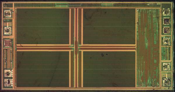
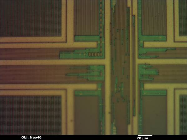
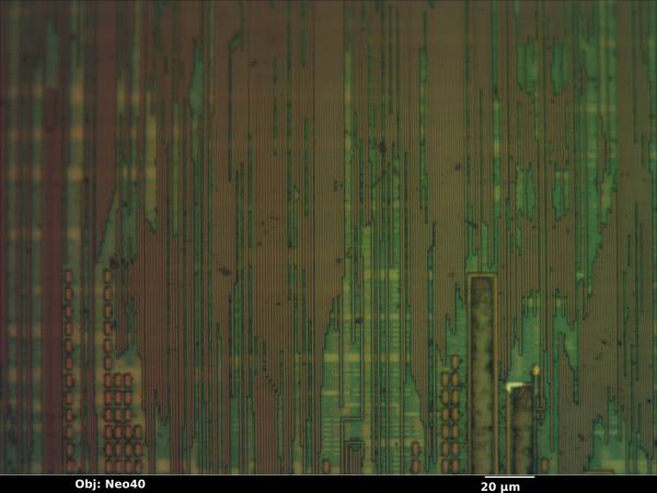
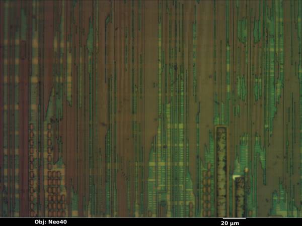
SPI serial SRAM chip. Looks like 4 metal layers and a fairly fine process geometry.
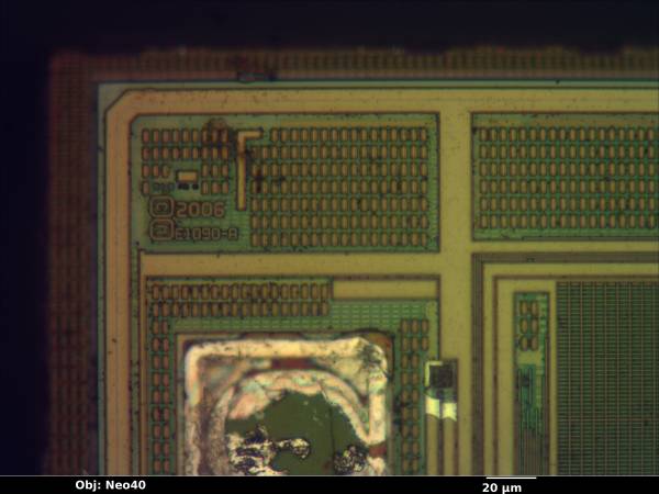
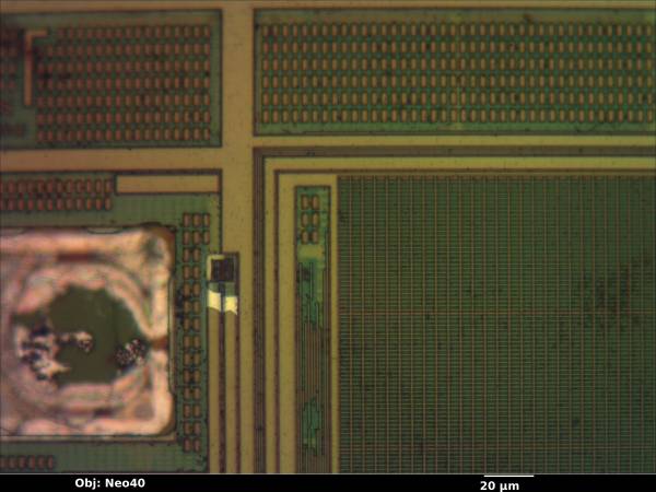
Definitely not one of Microchip's standard fab processes. CMP filler pattern is consistent with UMC 180 nm (pitch and dimensions of CMP filler and traces on both M4 and M3 match xc2c32a within 3%) however this is the only evidence we have to support this conclusion at this time; tag is tentative.
The die ID also does not match the normal Microchip layout and there is no Microchip logo on the die. Maybe this mask set was acquired from a buyout or something?
There are three unbonded pads on the die. Purpose of these is unknown at this time since all known packages are 8 pins.
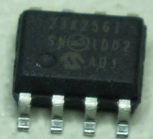
Package
Die
azonenberg/microchip/23k256.txt · Last modified: 2015/01/04 22:50 by 127.0.0.1

