Table of Contents

This page describes various chemical solutions applied to ICs for various effects. Primary reasons:
- To see lower levels (delayer)
- To differentiate doping (“staining” aka “decoration”). Applications include:
- Differentiate NMOS/PMOS transistors
- Optically read ion implanted ROMs
- To diagnose defects (“defect etching”). Not a focus here but some info
The etchant is sometimes called a corrodent. Miller indices (eg: {111}) are used to denote crystal properties. Many of these solutions have strong temperature dependencies.
Some solutions are used for more than one purpose. They are in the area most associated with them or at least of the most use on this site.
Open questions
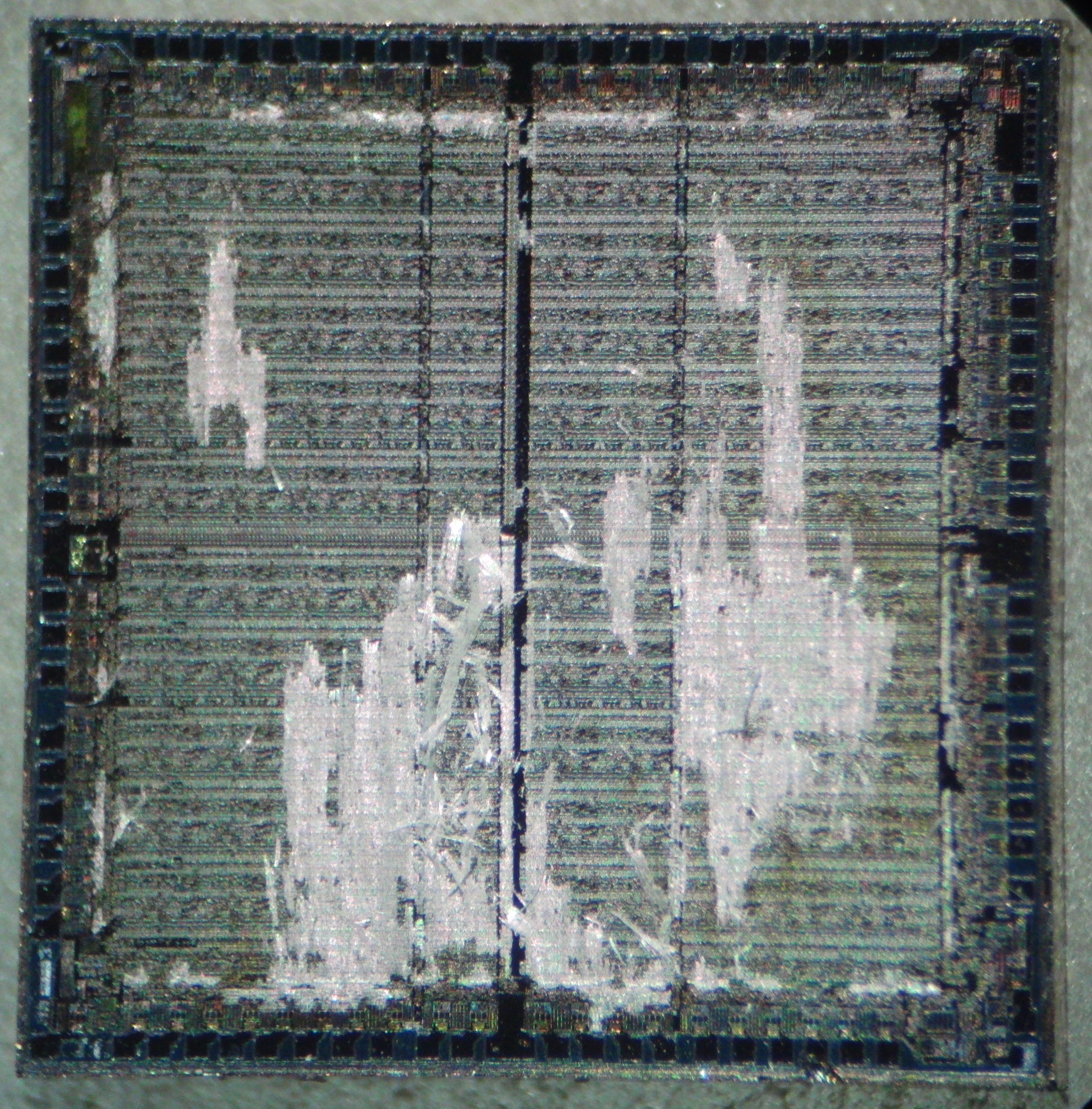
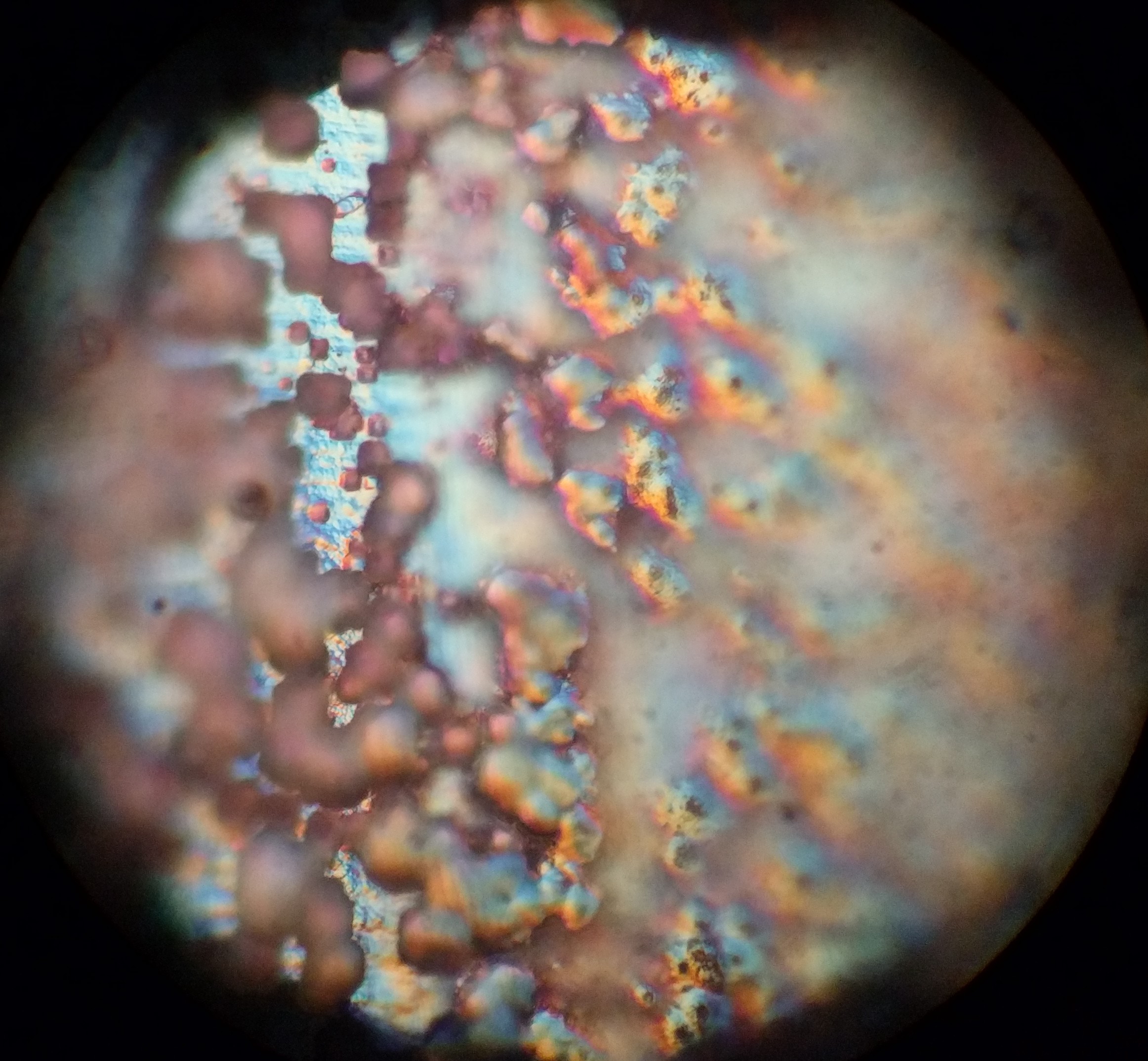
When I etch chips far down with HF some sort of crud builds up. What is it? Can it be prevented? Can it be removed? TODO: add picture
General notes
Hydrofluoric acid (HF)
Many of the solutions on this page involve this chemical. It is extremely dangerous and should only be handled if you know what you are doing. See site disclaimer on main page. If solution is sufficient concentration you will die a horrible death if it spills on you. That said, < 3.0% or so solutions are sold over the counter to consumers in the US as certain types of rust removers (ie one would hope its reasonably safe). The same solutions are banned for over the counter sales in the EU.
HF eats glass. Avoid using glass containers as they will get eaten and influence the etchant concentration, making etching less predictable. Polypropylene (PP), fluoropolymers (PTFE, PFA, FEP, ETFE, etc), and HDPE are all HF and acetone resistant. Of these PTFE and PP are the best. See corrosion data here and here.
Importance of cleaning
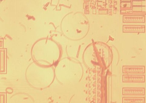
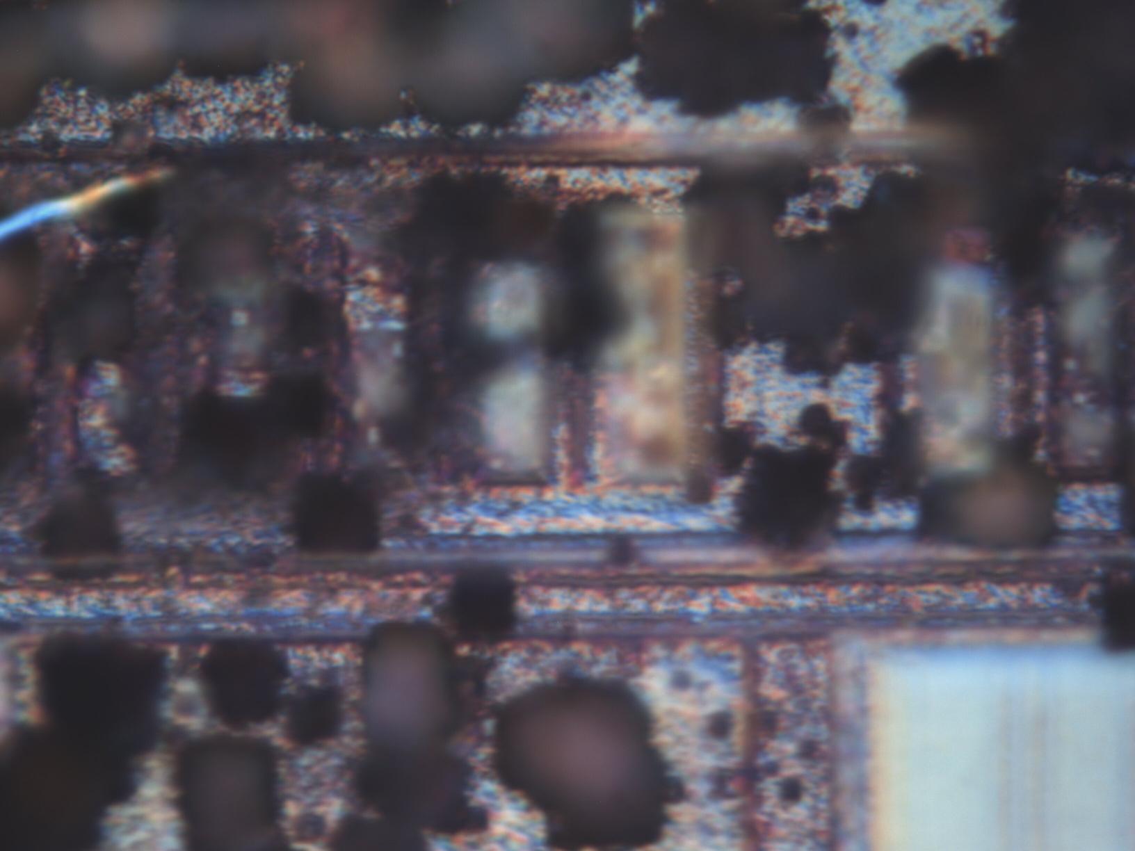
Dies must be clean before etching. If they are dirty (ex: oil patch) the etching will be very uneven. Above: SiO2 skeleton leftover from contaminated areas blocking etchant
Ultrasound
Generally speaking, ultrasound can really help etch reliability / smoothness by remove debris (see above) and by circulating solution to ensure even concentration.
Delayering for netlist extraction
An easy way to get good images from chemical etches (if multiple samples are available) is to throw a bunch of chips in the tank and take them out one at a time. This will allow different layers to be visible. If only one (or very few) samples are available the only option is to etch for a few minutes, then remove/rinse the specimen and inspect under a microscope to decide whether more etching is necessary.
Transistors
[bold-tech.com: Silicon Dioxide Etch] indicates that when using BOE, doped regions etch faster than non-doped regions.
ROM
See this page for background on ROM construction.
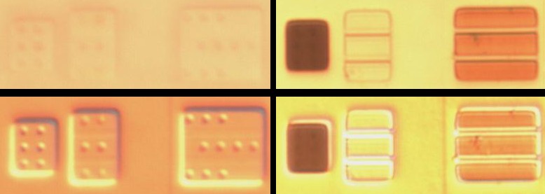
Ion implanted ROMs cannot be optically read by simply looking at top metal. However, they can be etched selectively (ex: contact based) or stained (ex: implantation) to be made visible.
“Smartcard 99” says: “The implant-mask layout of a NAND ROM can be made visible by a dopant-selective crystallographic etch (Dash etchand [Bec98]). This image shows 16×14 bits plus parts of the row selector of a ROM found on an MC68HC05SC2x CPU. The threshold voltage of 0-bit p-channel transistors (stained dark here) was brought below 0 V through ion implantation.”
Neviksti's comments on “DSP-1” page: “The Dash etchant worked for the NOR implantation rom (not the NAND rom, the opposite of what the paper claims). Which makes me wonder if they accidentally mentioned something else / mislabelled / whatever” (the paper being above quote from “Smartcard 99”). JM response: I've successfully stained NAND implant ROM. I haven't come across any NOR implant ROM yet
Determining sample thickness
Many solutions give distance per minute. Other than carefully observing when done, its useful to get some estimates to as how long etching takes. A couple of techniques:
- Focus on different layers and measure how much focus knobs had to be turned
- Use thin film interference colors: https://web.archive.org/web/20170324225827/http://www.idea2ic.com/LM13600/SiO2_Color_Chart.pdf
Observation
Generally speaking its difficult to observe these solutions directly while etching for several reasons:
- These solutions eat microscope objectives (mind vapors, not just the liquid)
- Bubbles can rise from the solution, obscuring observation windows
- Solution causes optical distortion. Additionally, bubble and evaporation cause the solution to change height and may require refocusing
The easiest way to get around these is to cover a microscope objective in Saran wrap. This allows the bubbles to pop and provides some fume protection. I still wouldn't do it with an objective you care that much about. This does degrade quality a little though. I've considered gluing a cover slide over but haven't tried it. In general I'd avoid direct observation (ie dip and check) unless you have a very good reason.
If checking samples under a microscope be sure to clean them thoroughly first. The hot microscope light will boil off any remaining solution leading to further unintended etching and possibly corroding your microscope. Be especially careful when etching metal layers as solution likes to hide under overhanging SiO2.
Anisotropy
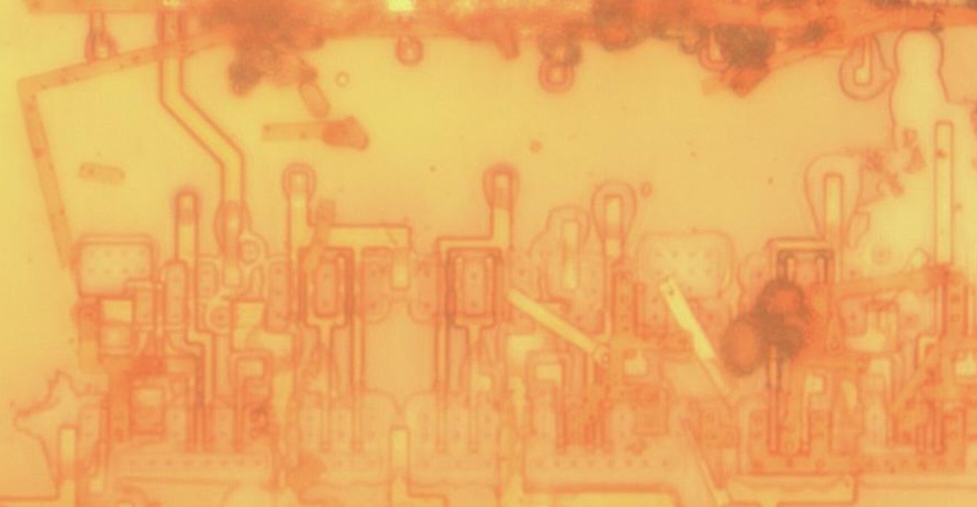
Above left: metal floating off during HF etc. The SiO2 under it was completely eaten. Right: polysilicon gates that floated off after the SiO2 was undercut.
An isotrophic etch removes materially equally in all directions. Most wet etches are isotropic because they remove any material they touch at constant rate. However, monocrystaline Si has planes that can be exploited to achieve some anisotropic etching. If you truly need anisotropic etching you should instead use RIE. That said, reasonably good results can often be had by etching to just where the metal stops and then etching away the metal with a separate solution. However, wet etching tends to be less consistent than RIE which still limits its use.
The isotrophic nature of wet etches generally limits wet etching to large feature sizes [JM experience, “Tools and Techniques” 149]. One thing to watch out for is beginning to undercut lower metal layers early from etching through vias. This can cause entire metal segments to lift off. Newer processes have this issue less because they use tungsten vias which tend not to etch as easily. [“Tools and Techniques” 148-149]
TODO: could we project light to achieve some degree of anisotropicity on the exposed surface? Unfortunately this has the best chance of working on Si (solutions are known to be photo-sensitive) where as this is mostly of interest on SiO2
Chemistry background
Silicon does not react with HF or many other things. Therefore, mixtures are used to create intermediates that can be processed. Having an understanding of this process helps to understand rates and how the mixture will react to different materials.
Oxidizing silicon to silicon dioxide
Silicon does not dissolve in most acids, including HF by means of the acid itself. However, oxidizing agents such as nitric acid convert it to silicon dioxiide [Friedrich Beck]:
3 Si + 4 HNO3 ⇒ 3 SiO2 + 4 NO + 2 H2O
Thus, exposed layers of elemental silicon are converted to silicon dioxide. Other oxidizing agents are potassium permanganate, hydrogen peroxide, iodic acid, and more.
Etching silicon dioxide
Usually we don't want just silicon dioxide but rather to remove it entirely. The most common way to do this is with HF [Friedrich Beck]:
SiO2 + 6 HF ⇒ H2SiF6 + 2 H2O
Don't recall any other SiO2 removing agents.
Dilutant
TODO: need more information on these
Using concentrated solutions, etch rates are typically too high. This means you have little reaction time and selectivity also tends to go down. There are three common dilutants: glacial acetic acid, water, and glycerine. Although water is readily available, it seems it is not preferred due to corrosion effects. Acetic acid is a liquid acid and glycerine is probably for when the pH should be kept more neutral.
Boron and Si
Tends to form borosilicate (which etchants?). Stops etching if boron concentration exceeds 1019 / cm3. [Wet-chemical Etching of Silicon]
Alkali etching
The idea is convert the silicon to silicate by using a liquid alkaline solution. Example reaction [Friedrich Beck]:
Si + 2 KOH + H2O ⇒ K2SiO3 + 2 H2
XXX: what if we used molten KOH? Maybe it wouldn't wash products away.
Optical
Optical excitation generates electronic by ejection?
Electrochemical
Putting positive voltage on Si in HF solution generates holes. [Fundamentals of microfabrication: the science of miniaturization]
Removing SiO2
HF
Straight HF will tear through Si quite readily
HF by itself will selectively etch SiO2 and various other compounds much faster than Si. Whink rust remover is an over the counter source of 3% HF (maybe 2% +/- 1%). HF can be synthesized from other chemicals, but is highly not recommended due to the extreme toxicity. For a chemical description of this reaction, see [bold-tech.com: Silicon Dioxide Etch]
Why use: selectively etch SiO2 over Si
Advantages
- Simple
- Can be used in combination with photoresist or similar masks to selectively remove filler over flash, etc. while preserving remainder of circuit
- Materials may be readily available (as off the shelf rust remover)
Disadvantages
- Solution can become depleted in certain areas leading to uneven etching
- Materials may not be readily available in some areas
- Metal layers may leave “shadows” in the oxide below
- Concentrations and time must be monitored to get good slices of the die
NOTE: HF eats aluminum. This can be good or bad depending on the application. A quick search shows that HF only eats Cu with an oxidizer present (ie typically slightly so from atmosphere)
2.5% HF will require some heating to etch. Heat it but don't reach boiling as the fumes are still dangerous. It still various considerably from chip to chip, but expect etch times in the range of 20 minutes to get through the top passivisation and then maybe 2 or 3 minutes a layer after that. If in doubt do only very small runs at a time (< 30 seconds).
Example procedure
Procedure
- Place die(s) in a plastic tray (see notes at top of page)
- Add 3% HF to each specimen until top is completely covered
- Wait 5-15 minutes, remove with plastic tweezers, and rinse
Alternate procedure
- Place small beaker (10mL is ideal) of water on hot plate, heat to near boiling
- Place die in plastic centrifuge tube
- Apply ~1mL of 3% HF to tube, cap, place in water bath for heating
- Remove from heat after 30 sec, suction HF with pipette. Rinse, inspect, and repeat if necessary.
Ammonium bifluoride (NH4HF2)
This essentially gives off HF when dissolved in water.
Buffered oxide etch (BOE)
More stable etching of silicon dioxide (SiO2) or silicon nitride (Si3N4) over, say 49% HF. Mixture [wiki: Buffered oxide etch]
- Ingredients
- 40% NH4F in water (6 mL)
- 49% HF in water (1 mL)
- Temperature: 25 C
- Rate
- Si (“thermally grown oxide”): 2 nm / s
- SiO2: unknown
- Notes
- Adding HCl may reduce insoluble oxide bi-products
Pitting
A common issue seems to be pitting if left in too long. As BOE itself can't etch silicon, it must be an additive. Some evidence suggests this is caused by not cleaning upper (ie metal) layers away. Possibly due to atmospheric oxygen. This also causes issues for staining and similar processes.
Recommendation: use phosphoric acid etc to remove upper layers completely before exposing silicon. Clean die and use fresh BOE solution.
Below example is on Generalplus GPLB52A24A
Above: left 40 min etch, right 40 hour etch 130F forced air w/ BOE
Above: die at angle, left side lower than right. Right side shows deep pits in focus even though its higher than surface visible at left
Above: deep staining shows doping much higher than substate now as evidenced by significant focus difference
Staining
General notes
Most reactions are quoted to work better with a strong cold light. This evidently favors the decorating reaction over other side reactions. I haven't done a study to see how much this really matters.
Dash etch
Good general purpose etching mixture to differentiate p and n doping, reveal implanted mask ROMs, and also has uses in failure analysis.
Staining Etch [Beck 74, 147]
Colors p-doped regions brown.
Advantages:
- Can show depth of p-doped regions
Disadvantages:
- High HF content causes strong SiO2 and polysilicon etch
General notes:
- Adjust concentration based on expected doping level
Mixture: “Concentrated solutions are used to investigate weak diffusions, e.g. well diffusions, while dilute solutions are used for strong dopings” [Beck 147]. XXX: why are the concentrations opposite? Use 30-200 mL (48%) HF to 1 mL (65%) HNO3.
SD 1 etchant [Beck 73, 142]
When to use: “…the most suitable of all the crystal etchants for the joint display of doping areas in n-silicon”
Advantages:
- Does not need to be made freshly
General notes:
- Improved result when light present (accelerates process)
- n becomes more rough than p
- Not selective to orientation planes
- This mixture will not show very strong: crystal defects, epitaxial layers, or oxide structures
Procedure:
- Mix ingredients
- Etch for 120 seconds
CP 6 etchant [Beck 73, 142]
When to use: when need to see both epitaxial and p-doped regions. “The etchant has proved particularly valuable for determining the position of the pn junction in power semiconductors”
Disadvantages:
- Must be made freshly
- Does not show crystal defects
- Can show epitaxial layers but short etch time makes it difficult to use? (“epitaxial layers can be represented, but the etching times for this are very short”)
General notes:
- Improved result when light present
Mix:
- 31 mL 65% HNO3
- 18 mL 10% Cu(NO3)2
- 8 mL 98% HAc
- “add 1.8 mL bromide per litre to this solution”
Procedure:
- Mix ingredients
- Etch for a few seconds
HF, Nitric, Acetic (HNA)
The most general purpose solution. Mixture
- Ingredients
- Glacial Acetic Acid: 11 mL
- 70 % Nitric Acid: 7 mL
- Hydrofluoric Acid 49%: 4 mL
- Temperature: unspecified
- Rate
- SiO2: unknown
- Si: unknown
Si
These are generally more useful for fab than anything else but are included here for completeness.
Tetramethylammonium hydroxide (TMAH)
WARNING: large TMAH exposure can cause sudden death
Mixture [Wet-chemical Etching of Silicon]
- Ingredients
- 25 % TMAH
- Temperature: 80 C
- Rate
- Si
- 37 (100) : 1 (111)
- 68 (110) : 1 (111)
- (100) Si: 0.3 - 1 um / min
- Si3N4: < 0.1 nm / min
- SiO2: 0.2 nm / min
- Notes
- Weakly anisotropic
Mixture [Wet-Chemical Etching and Cleaning of Silicon]
- Ingredients
- 20 % TMAH
- Temperature: 79.8 C
- Rate on Si (see source for detailed table)
- (100): 0.604 um / min
- (110):1.114 um / min
- (210): 1.154 um / min
- (211): 1.132 um / min
- (221): 1.142 um / min
- (310): 1.184 um / min
- (311): 1.223 um / min
- (320): 1.211 um / min
- (331): 1.099 um / min
- (530): 1.097 um / min
- (540): 1.135 um / min
- (111): 0.017 um / min
Ethylenediamine pyrocatechol (EDP)
Mixture [Wet-chemical Etching of Silicon]
- Temperature
- ? % EDP
- Temperature: 110 - 115 C
- Rate
- Si
- 20 (100) : 1 (111)
- 10 (110) : 1 (111)
- (100) Si: 1.25 um / min
- Si3N4: 0.1 nm / min
- SiO2: 0.2 nm / min
- Notes
- Toxic
- Weakly anisotropic
- Doesn't attack metals?
FB polysilicon etch 1 [Friedrich Beck]
Polysilicon selective etch solution. Mixture
- Ingredients
- 65% nitric acid (35 mL)
- 40% HF in water (1 mL)
- deionized water (14 mL)
- Temperature: room (25C)
- Rate
- Polysilicon: ~550 nm / min
FB polysilicon etch 2 [Friedrich Beck]
Polysilicon selective etch solution. Mixture
- Ingredients
- 65% nitric acid (16 - 26 mL)
- 98% acetic acid (12 - 23 mL)
- 40% HF in water (1 mL)
- Temperature: 20C
- Rate
- Polysilicon: ~150 nm / min
- Notes
- Requires constant stirring
- Do not reuse solution
- Selective against SiO2
FB polysilicon etch 3 [Friedrich Beck]
Polysilicon selective etch solution. Mixture
- Ingredients
- 65% nitric acid (2 mL)
- DI water (60 mL)
- 40% HF in water (3 mL)
- Temperature: 23C
- Rate
- Polysilicon: ~150 nm / min
- Notes
- Requires constant stirring
- Must be used fresh
- Selective against SiO2
Potassium hydroxide, alcohol
Isopropyl alcohol based [Wet etching of silicon]
- Ingredients
- Isopropyl alcohol: 60% by weight
- KOH: 40% by weight
- Temperature: 80°C
- Rate on Si
- (100): 600 nm / min
- (110): 100 nm / min
- (111): 6 nm / min
- Notes
- May require heavy stirring, tends to separate
- Isoproyl alcohol moderates / slows down reaction
Methyl alcohol based [Wet etching of silicon]
- Ingredients
- Water: 100 g
- KOH: 50 g
- Methyl alcohol: 40 g (30 mL)
- Temperature: 50 - 60C
- Rate for Si
: these rates seem too high, but thats what the page says. Maybe missing a u?
- (100): 0.7 m / min</span>
- (111): 0.035 m / min</span>
- (110): “roughly 4 times that of the (111) direction”</span>
- Notes
- Suggests reflowing, especially since otherwise concentrations get out of proportion
- KOH reactions with Si to produce H2, bubbles indicate damage in SiO2 if not expecting at given location
Applications
- Anisotropic etch
Potassium hydroxide, water
Mixture [Friedrich Beck]
- Ingredients
- KOH (? mL)
- Water (? mL)
- Temperature: 60°C
- Rate
- 510 nm / min
- Notes
- Use fresh solution
- Forms crystal patterns around exposed silicon, can be used to gauge effectiveness of solution
- Careful not to overetch
Etch rates vary dramatically with temperature and concentration. Higher concentrations do not always etch faster, but may give a smoother etch.
Negligible attack on SiO2 and silicon nitride [http://cleanroom.byu.edu/KOH.phtml]
Pyrocatechol, an amine
“Etching by sequestering” [Friedrich Beck]
- Amine examples
- ethylendiamine popular
- Hydrazine works (but is not technically an amine?)
- Useful for etching monocrylstaline
- Add pyrazine and water for related mixture
- Rate: relatively slow
Schimmel etch
Based on Secco etch, supposedly better.
Mixture [Wet-Chemical Etching and Cleaning of Silicon]
- Ingredients
- Solution (1 mL)
- CrO3: 75 g
- 1000 mL H2O
- 48 % HF (2 mL)
- H2O (0 - 1.5 mL)
Mixture [AIR LIQUIDE ELECTRONICS CHEMICALS & SERVICES, INC. SCHIMMEL ETCH]
- Ingredients (approx)
- HF: 34 parts
- CrO3: 5 parts
- Water: 65 parts
Secco etch
Mixture [Defect Etching in Silicon]
- Ingredients
- HF (2)
- H2O (1)
- K2Cr2O7: 44 g per (1)
- Notes
- Works on all all types of silicon.
Mixture [Friedrich Beck]
- Ingredients
- 0.15 M K2Cr2O7 (1 mL)
- 40% HF in water (2 mL)
- Temperature: unspecified
- Rate: unspecified
- Notes
- “According to [20] the mixture is appropriate, and even preferred, for grain-boundary structuring of polysilicon”
Seiter etch
Mixture [Defect Etching in Silicon]
- HF: 1 HF for 9 H2O?
- CrO3: 120 g per 100 mL of H2O
Etches defects very well on {100} surfaces, but nothing else
Sirtl etch
Mixture [Defect Etching in Silicon]
- HF: 1 mL
- H2O: 0.4 mL
- CrO3: 0.2 mL
Etches {111}, but nothing else. Chart shows results on {100} though, so not sure how true this is.
When to use it: “particularly suitable for displaying crystal disturbances in <111> silicon and produces large, sharply bounded etch pits in a short time…The preferred area of use for the Sirtl etchant is the display of stacking faults…, dislocations and sailing-boat faults” [Beck]
Advantages:
- “higher etch rate than other popular etch-pit corrodents” [Beck]
- “can be used to obtain sharply delimited etch pits with little surface disturbance on bare silicon surfaces with various crystal orientations in a relatively short time” [Beck]
Disadvantages:
- Does not keep / must be made fresh
Beck
When to use it: “particularly suitable for displaying crystal disturbances in <111> silicon and produces large, sharply bounded etch pits in a short time…The preferred area of use for the Sirtl etchant is the display of stacking faults…, dislocations and sailing-boat faults”
Chemistry (from Sirtl/Adler): 4 Cr + 24 H+ + 12 F- + 3 Si ⇒ 4 Cr+3 + 12 H2O + 3 SiF4
First add HF and then stock solution.
Stock solution
Mixture
- 25 g CrO3
- 75 mL DI H2O
Keep sealed after mixing.
Large etch pit
Mixture
- 1 mL stock solution
- 2 mL 48 % HF
Rate
- Dislocation substrate etch: 15 min
- Section decoration w/ light: 20 sec
- 1.3 um / min
Medium etch pit
Mixture
- 1 mL stock solution
- 1 mL 48 % HF
Rate
- Dislocation substrate etch: 15 sec to 10 min
- Section decoration w/ light: 10 - 20 sec
- 1.3 um / min
Small etch pit
Mixture
- 3 mL stock solution
- 2 mL 48 % HF
Rate
- Dislocation substrate etch: up to 10 min
- 1.3 um / min
Wright etch
Mixture [Defect Etching in Silicon]
- HF (concentrated) (1)
- CrO3 (0.5)
- H2O (1)
- HNO3 (0.5)
- Cu(NO3)2: 2 grams for 60 ml H2O
- 1 unit acetic acid
Why copper nitrate helps is unknown. Not sure what types of silicon this works on, maybe all.
Decoration as called by Fredrick Beck is the process of making parts stand out better.
Copper sulphate
Copper sulphate will bring out n-diffusion areas of pn junctions when illuminated (
Cu+2 + 2 e- ⇒ Cu
Si + 4 HF + 2 CuSO4 ⇒ SiF4 + 2 Cu + 2 H2SO4
At higher temperatures, HF etch takes over, so it needs to be done cold. In particular, do not use a hot light source such as a bare halogen lamp. If it goes through a microscope it should be fine as the thermal part should be heavily attenuated / distorted by the time it reaches the sample.
Periodic Acid Etchant
Good at showing where doping changes. Strong etch rate dependence on illumination. Room temp: mostly etches highly doped areas, especially p+ with max conc 1018 atoms / cm3 Increased illumination favors weaker doping.
- 20-50 seconds
- 50 mL H2O
- 5 g H5IO6 (periodic acid)
- 5 mg KI
- 2 mL 48 % HF
- Must be added in given order
Permanganate Etchant
3 mL KMnO4
97 mL 48 % HF
5.5 um / min on <111> @ 23C
Bichromate Etchant
Brings out n doped areas. Use 1:10 diluted Secco etchant. : H2O
Silicon etchant p
- 20 mL acetic acid
- 1 mL 40% HF
- 3 mL 65% HNO3
- 1-3 seconds
Staining etchant
- 12 mL 65 % HNO3 (works without nitric if just exposed to air?)
- 200 mL 48% HF
- 5-10 seconds
Doping etchants
These enchants are intended to be used to highlight either P or N
Many delayering solutions become increasingly structural as the light level increases. They are more selective at lower temperatures, so try to use a cold light, ie an LED and not a halogen. Of course, if you can put an IR shield, you can use a halogen just fine. Microscope optics might do this already.
Copper sulphate
Selective towards: n-Si
Mixture [Friedrich Beck]
Ingredients
- CuSO4 * 5 H2O: 8 g
- 48 % HF: 10 mL
- DI water: 980 mL
Rate: 5 - 30 seconds
Mixture
Based on above, but adjusted for off the shelf acid.
Ingredients
- CuSO4 * 5 H2O: 1 g
- 2.5 % HF: 24 mL
- DI water: 100 mL
Rate: 5 - 30 seconds
Calculations
- This is very approx, I don't know volume of HF and I assume its negligible
- wik says 1.15 g/mL for 48% soln
- Original: 48 g / 100 mL ⇒ 48 g
- Have: 2.5 g / 100 mL ⇒ 2.5 g
- 192 mL of 2.5 % for equal mass
- 990 mL original solution, - 190 mL ⇒ 800 mL of water
- Reduced by factor of 8
Metals
Al
Phosphoric
Beck reccomends 65% phosphoric acid to remove aluminum:
Ingredients:
- 65% H3PO4
Procedure:
- Heat acid to 50C
- Drop die into acid
- Cook until done
Notes:
- Rate: 0.2 mm/min
- Since a layer is rarely more than 2 um thick it should take just a minute to completely remove the layer.
- “Very uniform attack, also very gentle to oxides and silicon.”
- If you are having problems completely removing it there may be a metal barrier, see “Beck barrier Ti/TiN solution” (TODO: add pictures)
HCl-H2O2
Very aggressive. Use fresh solution, degrades quickly
Ingredients:
- 4 mL HCl
- 1 mL 35 H2O2
- 1 mL H2O
Source. They omitted concentrations. I put the ones I assumed they meant / what I've been using.
Nitric
Handbook of Corrosion Data, 542 says “At room temperature, the rate at which nitric acid attacks alloy 1100 exhibits a maximum at a concentration of 20%”. Take this as a baseline for
Ingredients
- Approx 20% HNO3
- 1 mL 70% HNO3 : 3 mL H2O
Procedure:
- Heat acid to 80C
- Drop die into acid
- Cook until done
Notes:
- How long?
Au
Aqua regia
Classic recipe. Will attack other stuff
Mercury
Works, but prefer solder due to health reasons
Solder
Use flux
Ti
Aqua regia does not react with Ti, use “Barrier Ti/TiN etch”
Barrier
Beck barrier etching solution
Mixture [Beck 45]:
- 9 mL 30% H2O2
- 2 mL NH4OH
- ~3 min @ 50-55C
Try to adjust for out of strong h2o2…
- 45 mL 3% H2O2
- 1 mL NH4OH
- unknown time
Notes:
- Reaction is exothermic and may heat up very hot. Moderate in water bath if having problems
- Seems to also react at room temp. You should be able to see more vigorous bubbling if its actually reacting. Its harder to see this at higher temps because the H2O2 will also decompose faster on its own
- Does not react with Ti?
Beck barrier Ti/TiN solution
Belive this is a more agressive version of above that also attacks Ti (and others?)
Mixture [Beck 45]:
- 200 mL 65% HNO3
- 1 mL 40% HF
- 20-25 @ room temp
Alternate:
- 1 mL Whink
- 10 mL 70% HNO3
Notes:
- 2023-07-23: did a good job near top metal when the other solution wasn't working
References
- AIR LIQUIDE ELECTRONICS CHEMICALS & SERVICES, INC. SCHIMMEL ETCH: http://alemis.us.airliquide.com/ChemSafe/MSDS/Image/114356_1.PDF
- bold-tech.com: Silicon Dioxide Etch: http://www.bold-tech.com/technical/silicon_dioxide.html
- Defect Etching in Silicon: http://www.tf.uni-kiel.de/matwis/amat/def_en/kap_6/advanced/t6_1_2.html
- Design Principles for Tamper-Resistant Smartcard Processors (Smartcard 99): http://static.usenix.org/publications/library/proceedings/smartcard99/full_papers/kommerling/kommerling_html/
- “Etch rates for micromachining processing” (“etch bible”)
- “Experimental investigation of anisotropic etching of silicon in tetra-methyl ammonium hydroxide”: http://spectrum.library.concordia.ca/141/
- Failure Analysis of Integrated Circuits: Tools and Techniques“
- Fundamentals of microfabrication: the science of miniaturization. Marc J. Madou.
- Integrated Circuit Failure Analysis: A Guide to Preparation Techniques. Friedrich Beck
- Isotropic Silicon Etching using HF/Nitric/Acetic Acid (HNA): http://engineering.tufts.edu/microfab/index_files/SOP/SiliconEtch_HNA_SOP.pdf
- “Manually” extracting a ROM: http://www.cherryroms.co.uk/forums/copier-and-hardware-forum/manually-extracting-rom.html?page=2
- Wet-Chemical Etching and Cleaning of Silicon: http://www.virginiasemi.com/pdf/siliconetchingandcleaning.pdf
- Wet-chemical Etching of Silicon: http://www.microchemicals.com/technical_information/silicon_etching.pdf
- “Wet etching of silicon”: http://www.microtechweb.com/kb/si_etch.htm
- Wikipedia: Buffered oxide etch: http://en.wikipedia.org/wiki/Buffered_oxide_etch
- “DSP-1 emulation”: http://board.zsnes.com/phpBB3/viewtopic.php?f=6&t=5868

