Table of Contents
Used for both decorating p areas as well as highlighting certain defects. In general, etch times are very short when used for decorating p areas (say 15 seconds) but it takes much longer to show crystallographic faults (say 12 hours). Can show epitaxial layers, doped areas and crystal faults [Beck].
Areas are initially stained brown (say up to 10 seconds). Longer exposures turns them blue. Beck says that strongly p-doped areas turn blue after 10-15 seconds [Beck 62] so I imagine that it really means they turn blue faster.
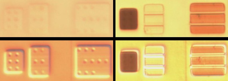
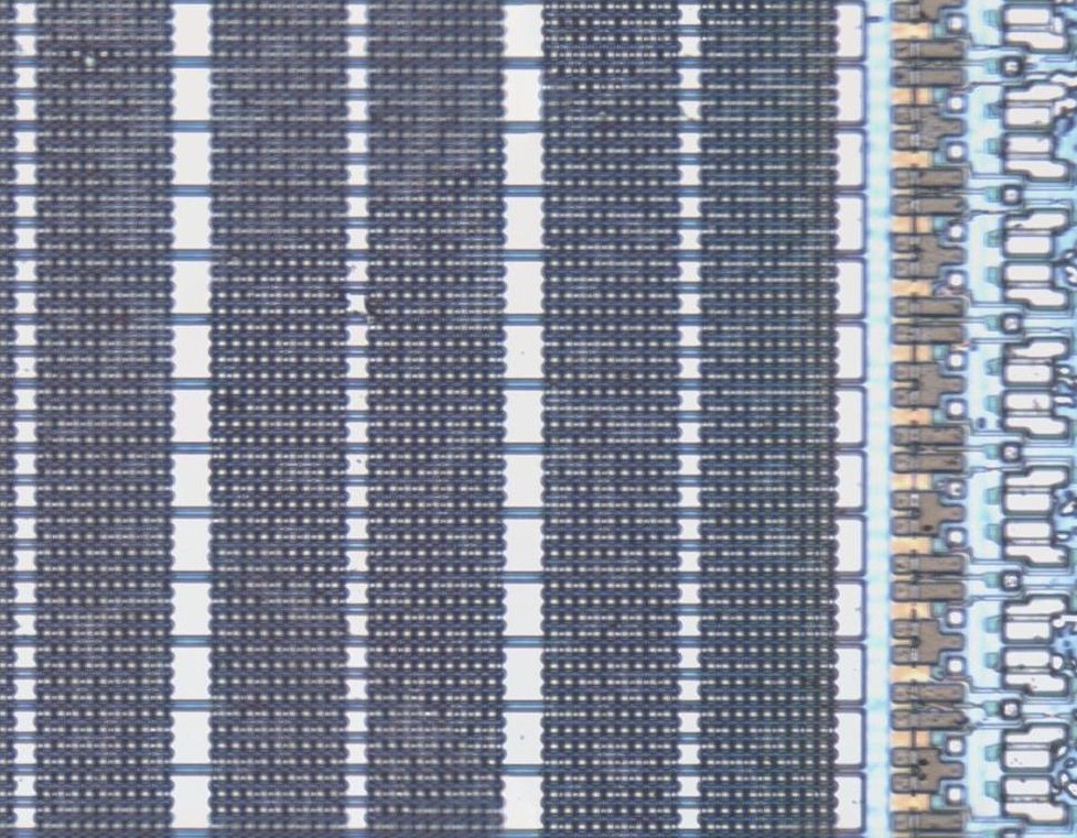
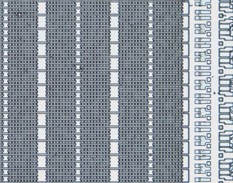
Above: samples before and after dash etchant. Left side: pre-etch, right side: post etch, top: brightfield, bottom: DIC. The original sample was visible only with DIC and P/N areas couldn't be distinguished. After decoration its clearly visible with simple brightfield illumination and DIC may now have made it less clear.
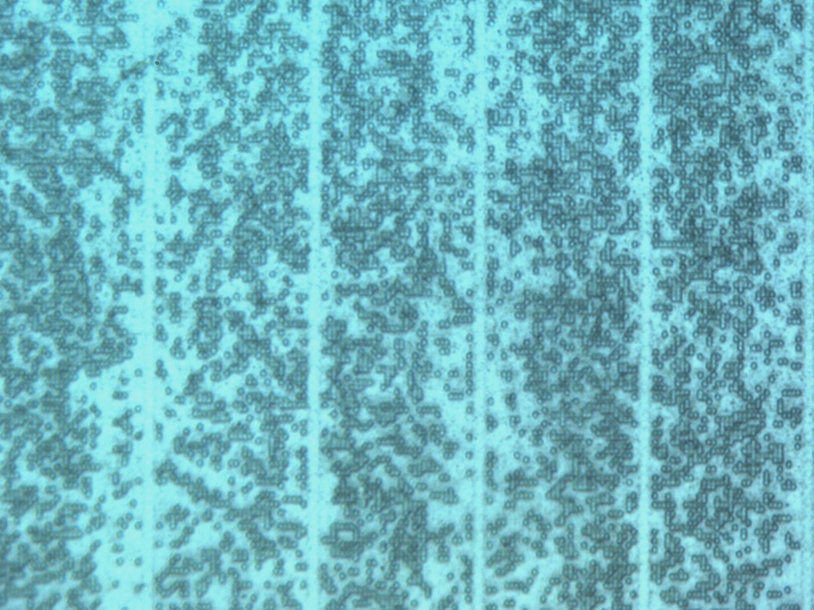
Above: left: unstained sample. Middle: light dash etching. Right: longer dash etching turns it blue-green.
WARNING: very temperature sensitive. I had a die sit for several minutes at 58C (in the garage) with no change. I then heated the solution (180F forced air, not sure actual temp) and after a brief exposure stained the die.
Theory of operation
The etch consists of hydrofluoric acid, a strong acidic oxidizer (typically nitric acid), and an acidic diluent (typically acetic acid). The basic reaction is similar to the classical HF + HNO3 isotropic etch for silicon: the silicon is oxidized, then the oxide is removed by the HF.
When the reaction is slowed down sufficiently (by dilution with a low-pH solvent which does not otherwise participate in the reaction) and the ratio of HF to oxidizer is within the proper range, an equilibrium is reached in which the rates of oxidation and oxide removal are essentially equal. P-type doping tips the equilibrium slightly in favor of oxidation, causing extra oxide to build up.
The resulting oxide can be seen optically in the form of thin-film interference (brown for thin layers or blue for thicker oxide layers) or observed with a SEM. In SEM imagery, P+ areas will show raised above the surrounding areas.
If STI oxide is removed with HF before the Dash etch, a three-level structure is formed, as seen in the image below:
For highlighting p regions
Use this to figure out of an area is N vs P stained.
“n-doped areas are scarcely attacked. p-doped zones are clearly brought out, and strongly p-doped areas change their colour from brown to blue after only 10-15 seconds…Epitaxial layers are also well shown.” Accelerated by light. Taking several hours, very slow / one of the slowest etchants. [Beck] For an example of staining ROMs see this
The chip should stain within a few seconds, 10-15 gives it plenty of time to make sure that everything sets well. However, the staining continues to change color with longer exposure so beware as n regions will also turn. It should be safe to ultrasonically clean the chip after staining if desired.
Equipment:
- 100 mL PTFE beaker. Other HF resistant plastics should also work
- 50 mL container to hold DI water
- Clock
- Plastic pipette
- Optional: bright cold light. Fiber illuminator should work, I use a a high output LED bicycle light
Consumables:
- 5 mL or so of Dash etch. I'm not sure how much is really needed but you should be able to comfterably cover the chip anyway
- De-ionized (DI) water
Procedure:
- Clean chip *thoroughly* (ultrasonic acetone-DI suds-IPA). Instead of dumping the IPA off and drying chip, instead rinse it with DI water. Do not let the chip ever dry out. Keep it submerged in DI water for the time being. If you suspect there is any grime on the chip you must clean it first or it will mask that region and may cause other complications. Using tap water suds may cause salt contamination, use de-ionized (DI) water
- Rinse out beaker and container with DI water
- Place chip on bottom of plastic beaker (I use 100 mL PTFE). Keep a few drops of DI water on it to keep it wet. They should stick with surface tension.
- Fill second container with 50 mL DI water
- Tilt beaker slightly with the chip on the raised side
- Pippette 5 mL Dash etch into lowered side of beaker
- Turn on bright light and point into beaker
- Watch clock to hit the minute mark (or other easily rememberable spot). Slowly turn beaker 180 such that Dash etch will creep onto the chip without flipping it over
- Let etch for 10-15 seconds
- Dump the DI water into the beaker
- Dispose of most of the solution in the beaker, making sure to not let the chip get dry. Wash the chip in the beaker a few times
- Vortex chip in beaker for a couple of minutes. Experience has shown that if not thoroughly washed acid traces can stay on the chip and it will etch/expose over the next few days, sometimes resulting in deep gouges
- Wash in IPA (ultrasound is safe) and blow dry
Notes:
- I'm currently using “Structural etchants” mix since I now have 48% HF. Other mixtures may work just as well, I haven't revisited them since I got better at cleaning the sample
- Tap water is not de-ionized!
- All solutions/equipment must be copper free: HF solutions will readily deposit copper on the die and create a pesky mask. Reccomend using a dedicated metal free beaker
Mask ROM staining procedure
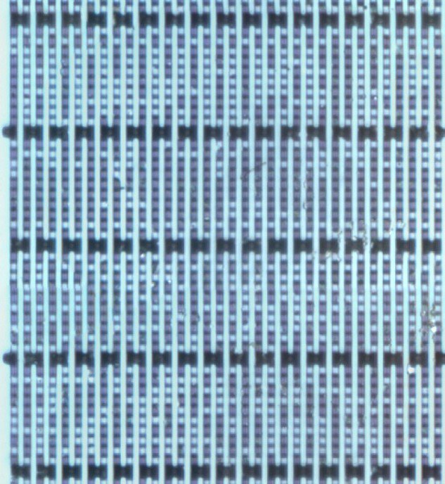
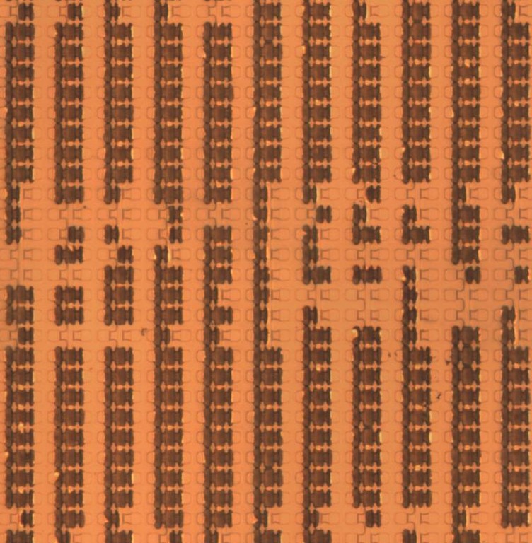
Some mask ROMs are implant programmed instead of, for example, using metal. While normal diffusion is very easy to see under a microsocpe, these active areas are not (easily) optically visible by themselves. See the mask ROM page for details.
It wasn't too hard to get some staining but required some rigor for reliable results. I re-iterate: this isn't too hard but requires a great deal more attention than a lot of the other procedures on this site: the sample must be handled much more gently and the etching is time sensitive. I'm guessing that the doping is done a little different way such that it is much shallower than others making it easily damaged. Not all of these steps may be necessary but each one helps to control specific risks. I reccomend you do the above “highlight p regions” procedure first to get a basic hang of things.
Important things:
- The sample must be very clean so as to not mask any etchants
- Do not apply delayering etchant for longer than need be. It seems to slowly etch Si and/or pull out ions fast enough that it will lead to poor staining if it comes in contact with the implant for too long
- Do not ultrasound the chip while delayering the ROM area. This causes things to break off more unpredictably and can lead to some areas etching a lot faster than others causing above problem to get worse
Equipment:
- 100 mL PTFE beaker. Other HF resistant plastics should also work
- 50 mL container to hold DI water
- Clock
- Plastic pipette
- Optional: bright cold light. Fiber illuminator should work, I use a a high output LED bicycle light
Consumables:
- Buffered oxide etch (BOE)
- 5 mL or so of Dash etch. I'm not sure how much is really needed but you should be able to comfterably cover the chip anyway
- I'm currently using “Structural etchants” mix since I now have 48% HF. Other mixtures may work just as well, I haven't revisited them since I got better at cleaning the sample
- De-ionized (DI) water
Procedure:
- Decapsulate chip through your method of choice. Metal damage probably won't effect results too much
- Clean chip *thoroughly* (ultrasonic acetone-DI suds-IPA). Instead of dumping the IPA off and drying chip, instead rinse it with DI water. Do not let the chip ever dry out. Keep it submerged in DI water for the time being. If you suspect there is any grime on the chip you must clean it first or it will mask that region and may cause other complications
- Rinse out beaker and container with DI water
- Perform delayer etch cycles until the ROM area has no more SiO2 on it. Make sure to read the delayer etch cycle notes below
- Place chip on bottom of plastic beaker (I use 100 mL PTFE). Keep a few drops of DI water on it to keep it wet
- Fill second container with 50 mL DI water
- Add 5 mL of BOE
- Vortex chip for 30 seconds (or longer if you are feeling adventuresome). Do not use ultrasound
- Dump the DI water into the beaker
- Dispose of most of the solution in the beaker, making sure to not let the chip get dry. Wash the chip in the beaker a few times
- Vortex in IPA and blow dry. Do not use ultrasound
- Inspect under microscope to see if ROM active area is exposed
- Fill second container with 50 mL DI water
- Tilt beaker slightly with the chip on the raised side
- Pippette 5 mL Dash etch into lowered side of beaker
- Turn on bright light and point into beaker
- Watch clock to hit the minute mark (or other easily rememberable spot). Slowly turn beaker 180 such that Dash etch will creep onto the chip without flipping it over
- Let etch for 10-15 seconds
- Dump the DI water into the beaker
- Dispose of most of the solution in the beaker, making sure to not let the chip get dry. Wash the chip in the beaker a few times
- Vortex chip in beaker for a couple of minutes
- Experience has shown that if not thoroughly washed acid traces can stay on the chip and it will etch/expose over the next few days, sometimes resulting in deep gouges
- Wash in IPA (ultrasound is safe) and blow dry
General notes:
- Because of the field oxide, it can be difficult to get both a good stain on the ROM as well as to stain the general active areas on the same chip. If you have only one sample, stain the ROM, photograph it, and then use HF to remove the rest of the Fox. Re-stain the chip and the active areas should stain but you might lose the ROM staining. You could try masking it if you were really determined
- If you over-delayer the chip it may not show up at first. You may still be able to get the data to show up, double the stain time and retry, giving up if you accumulate around 4 minutes
- I'm currently using “Structural etchants” mix since I now have 48% HF. Other mixtures may work just as well, I haven't revisited them since I got better at cleaning the sample
- Tap water is not de-ionized!
- Over-delayering by 1 minute will likely destroy the data. The lower you can keep that number the crisper the data will be
- All solutions/equipment must be copper free: HF solutions will readily deposit copper on the die and create a pesky mask. Reccomend using a dedicated metal free beaker
- Ultrasonic cleaning during the delayering step may cause areas to chip off leading to uneven etching. Vortexing also helps to keepp things even but is much gentler
- Try to do in 20C+ environment. I may have had some issues from HAc freezing in solution, keeping 20C+ should eliminate any concern
Delayer etch cycles notes
- Remove metal layers as they are exposed, probably ideally just as you begin to undercut them. Ideally they probably should be removed before the mask ROM is exposed
- Al: remove using phosphoric acid. See full Al section below especially for notes on metal barrier which may be more common in implanted chips
- Cu: haven't had to deal with it yet but it could be problematic since it will want to deposite on the Si
- Optimal time to stop delayering is usually just a little after the polysilicon is lifted off of the ROM area. Poly may still be attached to the line drivers, don't worry if it is, they aren't important. If you want its safe to ultrasound it at that point and they will get knocked off
- You really should use BOE over HF: BOE doesn't eat metal which prevents hard to remove AlF salts from depositing on the die
- If you are carefully watching it, you should see it change colors (when dry) and then turn clear once again which means its done
- Initially you can probably get away with longer cycles (maybe a minute or two) but make sure to turn it down to 30 seconds max at a time if its already been a few minutes
- Each round takes me about 10 minutes. I have lost a few chips to trying to save time by etching longer. Sometimes this saves time but sometimes it destroys the chip and is very frustrating. You are probably better off biting the bullet and just doing smaller cycles even if it takes you longer
- I experimented with trying to observe the etch under microscope but found it was more hassle than it was worth for various reasons
- There may be a large amount of field oxide left when its done
For crystallographic faults
When used for showing crystalgraphic faults, one of the oldest etchants and “not optimal in terms of selectivity and sensitivity”, 4-16 hours [Defect Etching in Silicon] When to use it: when you need good quality and can afford to wait up to a day. I (JM) have not had a reason to try this yet but its here for completeness.
Advantages:
- Very good selectivity
- Chromium free [Beck]
- XXX: what issue would Cr cause?
Disadvantages:
- Very slow (hours to near day)
: how does light intensity play into this?
Mixtures
The first is the recommended/standard mixture. The others are estimates at optimial mixtures using more easily accessible HF grades.
"Structural etchants" mixture [Beck 60]
Recommended mixture:
- 3 mL 65% HNO3
- 1 mL 48% HF
- 10-12 mL 98% HAc
Rate:
- (111) Si @ 23C: 2 nm / min
- Dislocation substrate etching: up to 24 hours
- Section decoration: 120 seconds with light
McMaster Whink mixture
Adjusted from above to have roughly same ratio HF to HNO3
Mix:
- 4 mL of stock solution
- 0.5 mL 65% HNO3
- 27 mL 2.5% HF
- 11 mL Hac
Gave poor results in trial run but I suspect this may have actually been from incomplete SiO2 etching.
McMaster RustGo mixture
Adjusted from Beck to have same solution concentration of HNO3 and HF, then remainder filled with HAc. The NH4F2 is ignored. Although I don't know if its optimal, I have gotten good results with this solution.
Mix:
- 3 mL 65% HNO3
- 4.3%
- 4 mL 12% HF
- 3.2%
- 8 mL HAc
- remainder
ROM
2019 new results
- Evidence that light is important for best result
- Used halogen fiber light
- Strong evidence that any metal during any HF-substrate step may ruin the result
- Workaround: always shine light on?
- Seems to etch through the doping
- Only good results using Dash. Not using any alternate mixtures
Played around with using lapping to more aggressively remove metal. Alternatively maybe do more aggressive phosphoric etching
Notes:
-
- Set to full power unless otherwise indicated
- mcmaster: dash staining done in PP container w/ die facing up. One light at top, one light on side
References
- Defect Etching in Silicon: http://www.tf.uni-kiel.de/matwis/amat/def_en/kap_6/advanced/t6_1_2.html
- Integrated Circuit Failure Analysis: A Guide to Preparation Techniques. Friedrich Beck

