“Explosive decap” is a tongue-in-cheek term referring to blowing a semiconductor device to bits (usually by accident). While this is rarely intentional, the remaining fragments can be interesting to study.
Mechanism of operation
The primary mechanism of explosive decap is the same as “popcorning” in BGAs: trapped water vapor in the packaging boils, has nowhere to escape, and ruptures the packaging with a small steam explosion. There is, however, one key difference: popcorning is induced by the soldering process (and typically is less dramatic in appearance due to the slower thermal gradients). Explosive decap, however, is much more rapid: common malfunctions such as short circuits or connecting power backwards will heat the device from room temperature to >Tjmax in a fraction of a second, causing much more vigorous fragmentation.
Small pieces of chip shrapnel may be thrown several feet in extreme cases.
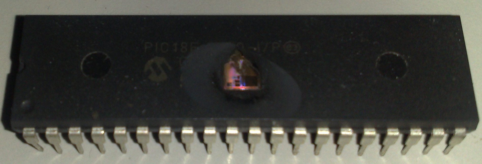
Explosive-decapped PIC18F4550 showing most of the die exposed (courtesy of Viper-7):
Example (7805 regulator)
This case involved connecting a TO-220 packaged 7805 linear regulator to a miswired (unprotected and polarity reversed) 11.2V Li-ion battery pack. The extremely low ESR battery voltage being dumped into what was effectively a forward-biased zener diode caused a massive thermal spike which blew the front half of the TO-220 across the room and exposed most of the die. A yellowish flash of light was visible as well, which may have been an incandescent fragment of bond wire or burning package fragment.
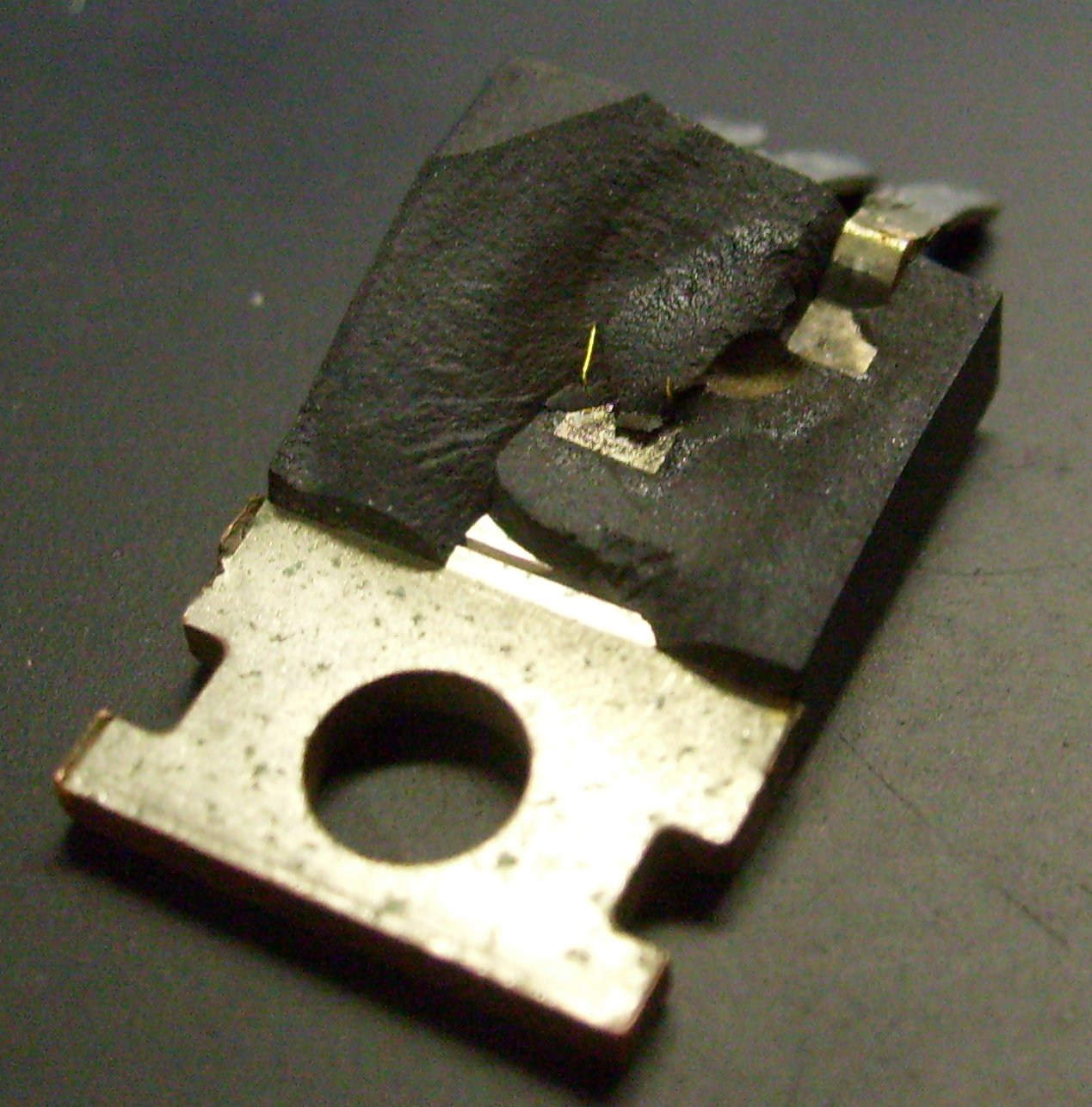
The remainder of the device after explosive decap with partially exposed die and leadframe. The rounded crater at upper right is most likely the location of of the original explosion.
Recovered package fragment. Note shell over leadframe at right side and blast crater just to the left.


