This is an old revision of the document!
Table of Contents
Also known as “plastic” packages
See also
Getting started
Probably the easiest to get a hold of is H2SO4. If you are in USA, you can easily buy it from https://www.dudadiesel.com/ Alternatively some drain cleaners (Liquid Fire brand) are concentrated H2SO4. Use this in combination with a heat gun in a test tube to be able to quickly heat up and decap ICs. Ideally get a temp controlled heatgun (ex: I use HG3002LCD) for better control.
Also buy some safety equipment such as latex gloves and a lab coat. H2SO4 destroys clothing and human skin. I also recommend a fume hood or a full faceplate respirator (ex: 3M 7800S) with acid gas cartridges.
If you can get slightly better stuff, I typically use WFNA in a vortexer with a heatgun pointed at it. I use Oak Ridge FEP vials. I used glass initially but it was chipping corners due to vortexing. WFNA with sufficient volume/temperature gives more repeatable results (occasionally H2SO4 corrodes dies, my WFNA setup never does).
A Dremel with cutting wheels is also desirable to cut down the packages. Also, HCl + H2O2 are useful to subsequently etch out the paddle.
If you get everything above you'll essentially have my decap setup.
Acid decapsulation
Reactive Ion Etching (RIE)
Gases are ionized near the surface to eat the chip away.
Solvent
Special solvents have been developed that more or less dissolve the packages.
Mechanical decapsulation
Thermal decapsulation
Hybrid decapsulation
Applying multiple techniques.
Plasma
Has some info: https://escies.org/download/specdraftapppub?id=3144
Trimming
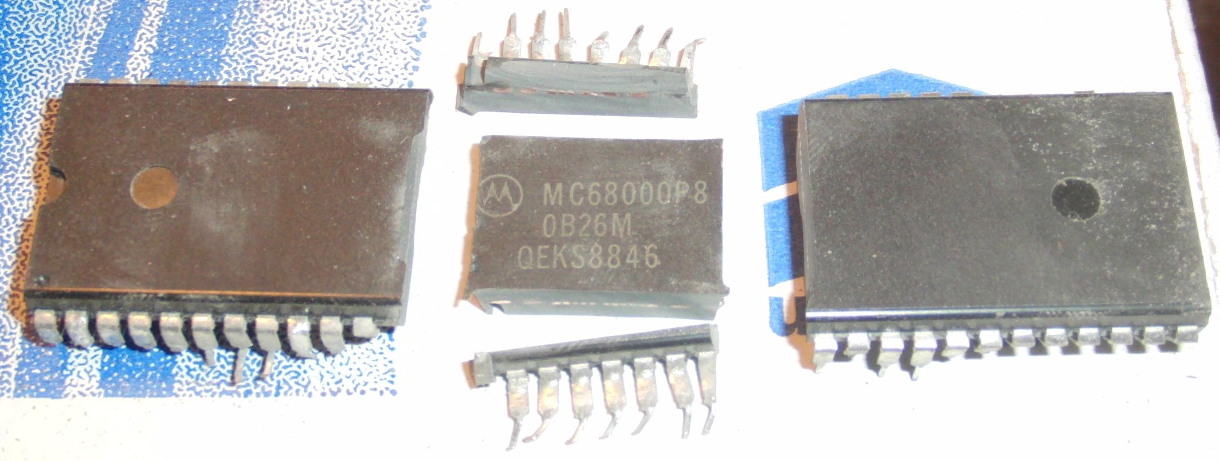
Sometimes large PDIPs only have a small die and lots of epoxy. The A perfect example is our friend the MC68000:
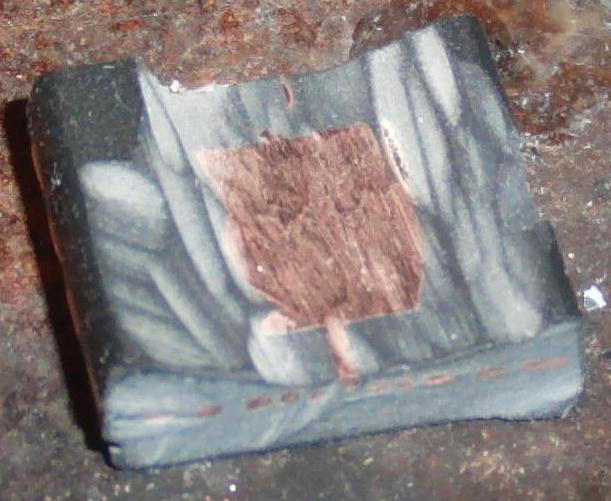
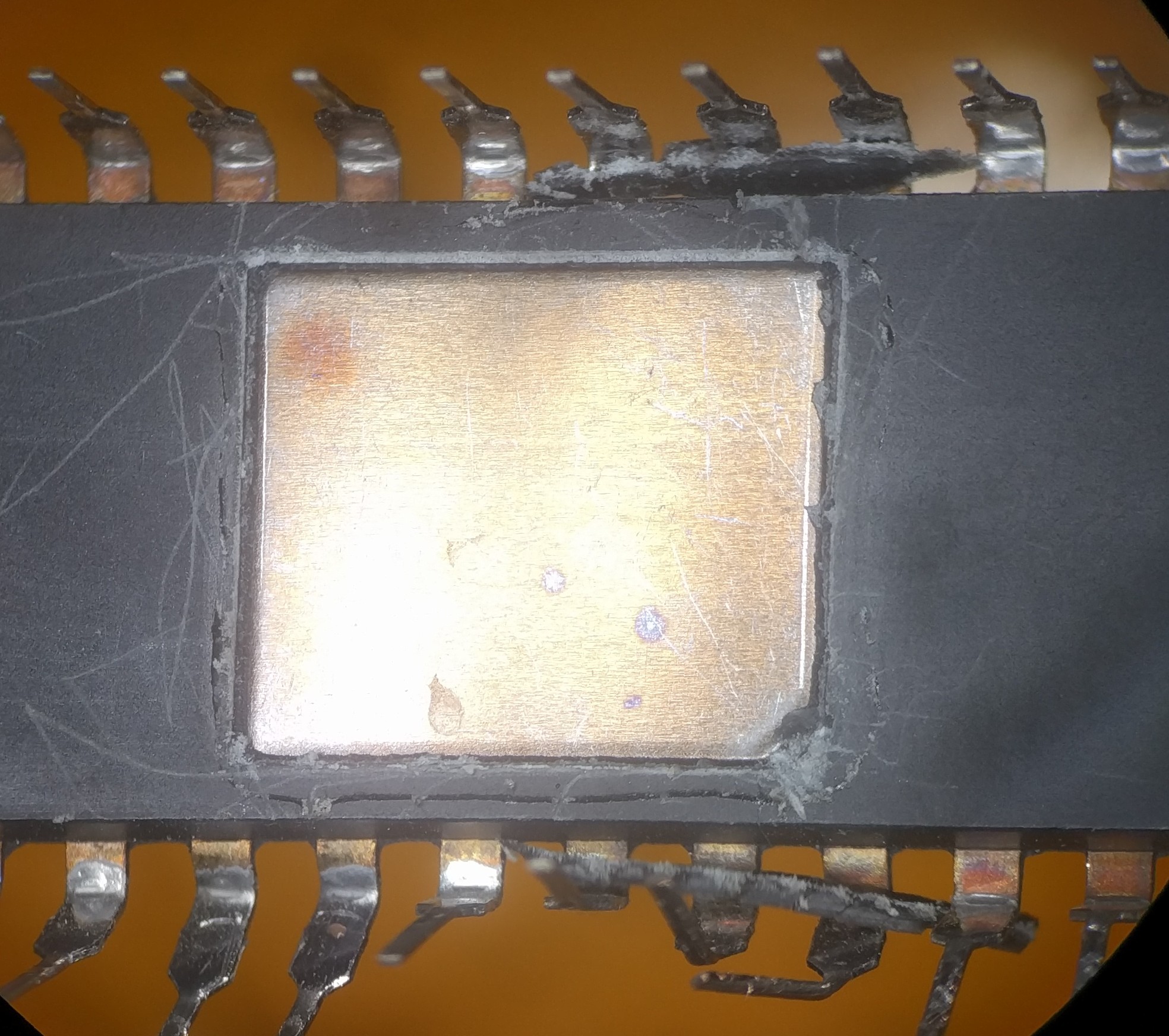
I used a Dremel (cutting wheel) to carefully scrape away the bottom of the package until the carrier island was visible. I then cut out the sides until the entire carrier island outline was visible:
And then cut it out:
I ended up trimming this much closer, maybe a few mm. My guess is you are safe as long as you don't touch the carrier island so get as close as your cutting skill permits. I repeated on a few specimens and none had any damage. In fact, I think they turned out better because they spent less time in acid waiting for the package to dissolve.
Of course, if it turns out to be a flip chip you're probably screwed as silicon would like not respond well to a Dremel bit. So, don't do this for a critical specimin but can save a lot of time and acid when the specimen is expendable.
Removing die paddle
Preparing for removal
Depending on the attach method, sometimes the paddle does not come off easily after decapsulation. Because this can be very problematic, it is reccomended to instead expose the paddle before decapsulating and then remove it chemically. I use doubled dremel cutting disks and make smooth circular motions to grind it down (note I mean grind, not cut). If the die was already decapsulated, place some CA glue on a small bit of paper towel and place the die face down in it. Press the die lightly into it. This should resist most of the chemicals here sufficiently for the time needed and is easy to remove. If you are really worried use epoxy and then remove with nitric acid.
Bulk removal
Most of the time the die attach paddle are common metals that can be removed by doing the following
Equipment:
- Acid resistant container with moderate heat resistance (small glass or PTFE beakers work good)
Consumables:
- 3 mL H2O2
- 3 mL HCl
Procedure:
- Add H2O2 and HCl to beaker
- Drop chip in. Should immediately begin to bubble
- Wait until furious bubbling stops, and then another minute to make sure the last scraps are eaten
- The heat will make it continue bubbling but it may not be dissolving anything
- If a pink residue is leftover, ultrasonic clean the die. It should come off within seconds
- If a gold residue is now leftover, boil in aqua regia for 10 minutes or until gone
Notes:
- Mixture will begin to decompose slowly self heat. Should be used within 10 minutes or so
- Consider cooling the beaker
Chip on board
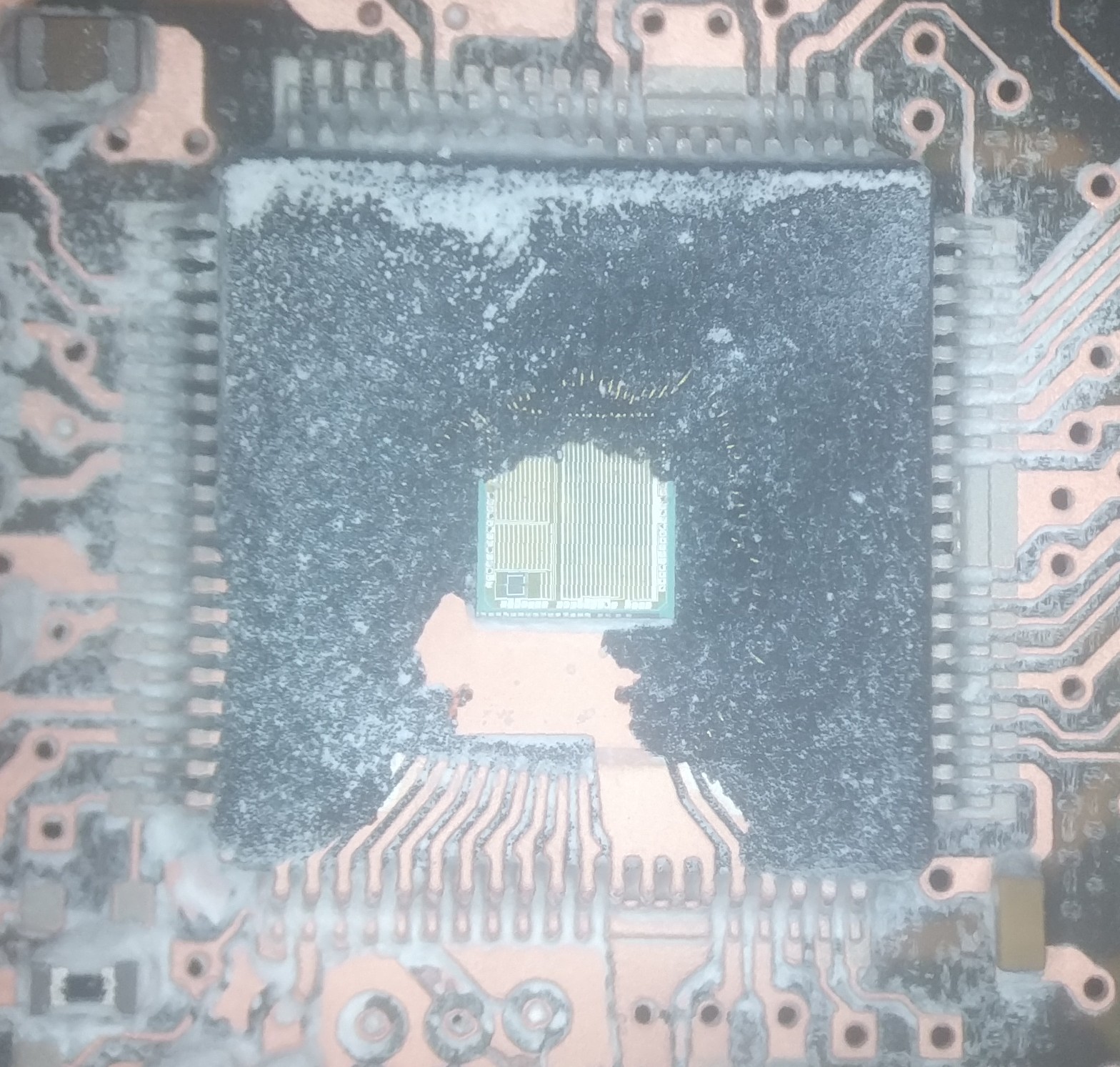
Usually when I decap a die I've ground the package down such that the bond wires are not tied to anything and come off with the chip. However, this is not easy with COB as its hard to determine where its safe to cut. Additionally, there is typically a mix of the epoxy circuit board combined with the epoxy blob on top of the ic. If you are adventuresome you may be able to remove the PCB (sand it off?) but I currently don't.
This leads to some challenges that you don't see with normal packages. For example, the die may still be held onto the circuit board even after the epoxy is removed. This prevents acid from flowing under it and dissolved it off. For this reason, I typically do COB decaps in several passes. After a few min of decap I stop and gently delaminate the PCB by removing loose layers. This allows acid to better get to the bottom of the COB to clean it up.
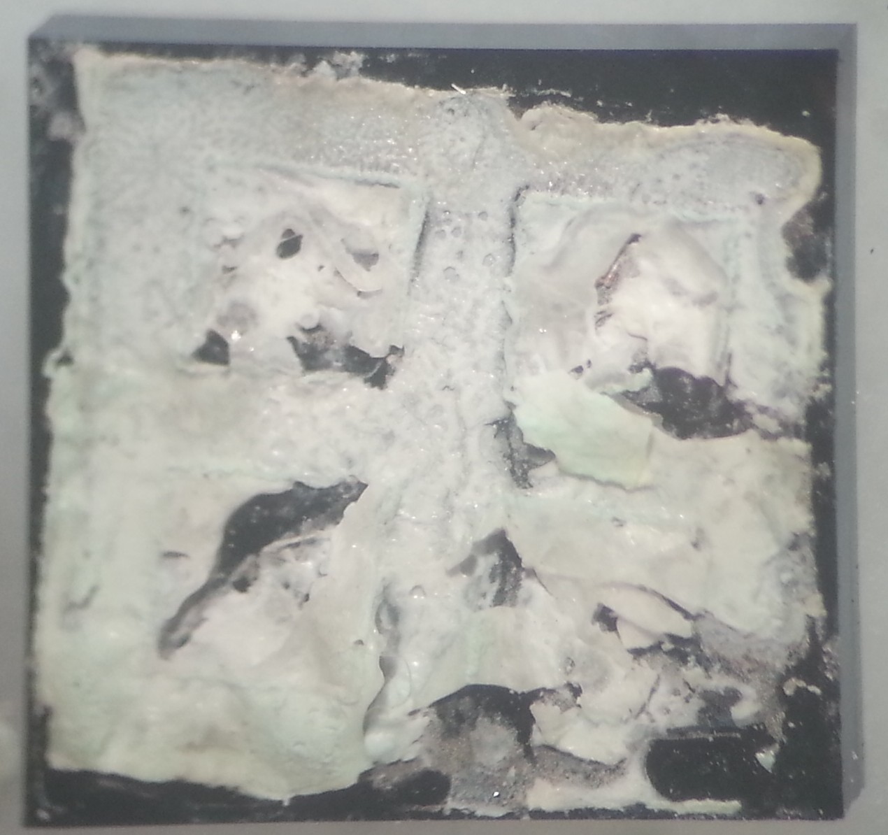
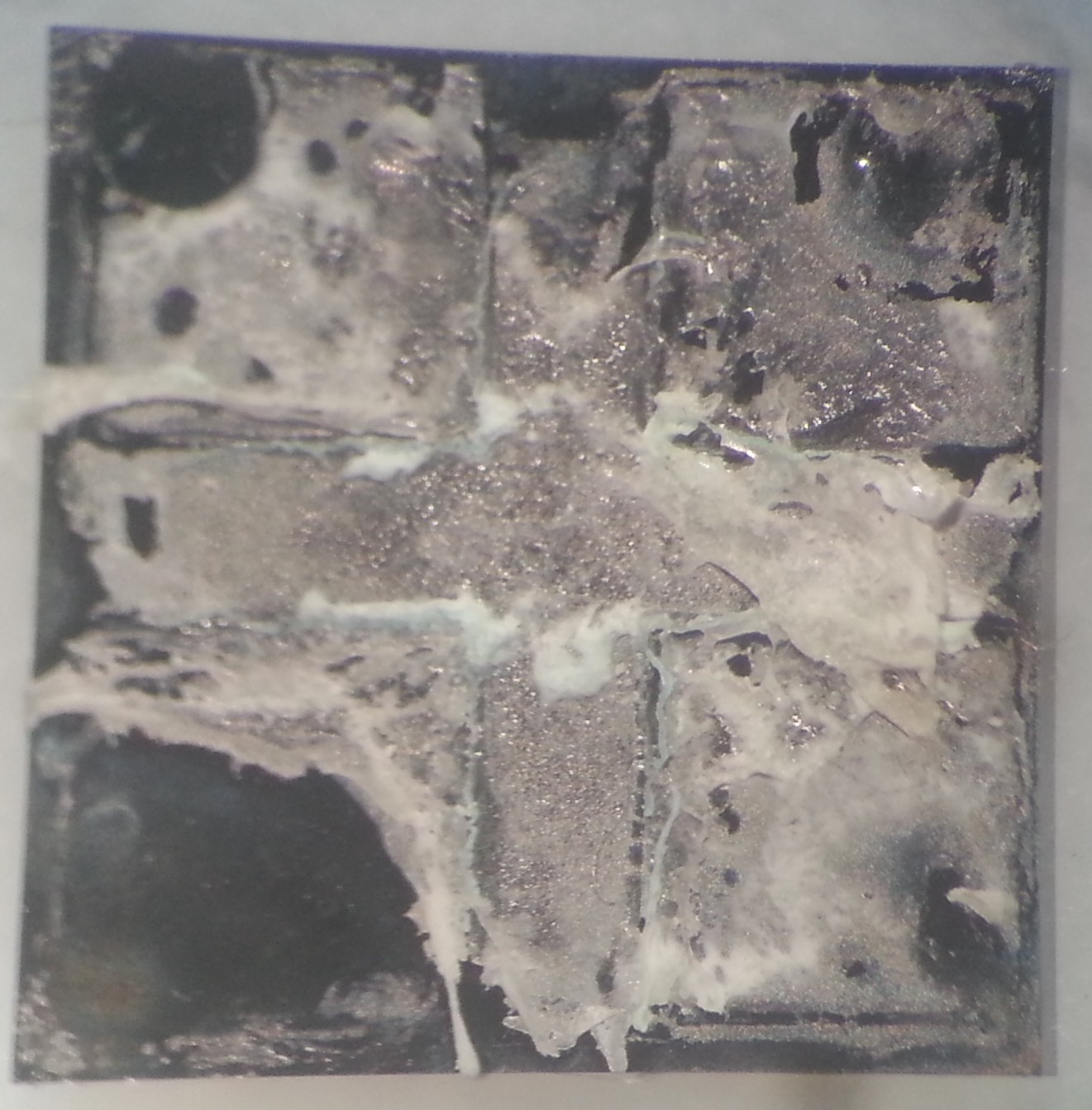
Above: bottom of some COBs after release. There appears to be a mix of silver epoxy and the remains of plastic sheets.
One problem from this lack of circulation is that it may create pockets of low concentration acid, leading to corrosion. The above dies were washed before that picture was taken to remove copper nitrate residue that had built up. It probably came from a paddle but may have come from the PCB. After rinsing with water, the bottom of the die was CA glued down. Then the back of the die was gently cotton swapped with acetone. Finally, the whole thing was soaked in acetone to release the die.
McMaster live 2019-11-10
Experiments trying to decap COB while keeping PCB intact
TLDR best result
- Cut a polypropylene tube (ie from a microfuge tube) roughly the size you want to expose to acid
- Heat tube up to soften it
- Warm PCB
- Attach hot tube to PCB, letting plastic deform into place
- Let cool a little
- Seal outside of tube with silicone
- Let silicone cure
- Decap with gentle heat on hotplate (maybe 160F max) using 2 WFNA : 1 H2SO4
Above is a compromise between PP providing the best chemical resistance and silicone providing the best seal
Silicone only experiment
- Made silicon dam by layering up
- Silicone surface cured, but internally didn't always
- Uncured silicone dissolved in WFNA and floated to top. This then cured and blocked the surface
- Interesting, but not what I was looking for
- Acid may eventually undermine the PCB, but eating the silicone itself came first
Someone also suggested I should try PTFE gasket. In the past I had tried kapton which didn't work well (acid tended to wick into kapton). Maybe PTFE would repel acid better
Live analysis considerations
Commercial “automatic” machines use a variety of techniques to etch the IC appropriately. One such technique is to seal off the area under attack using a chemically inert gaskit. See nitric acid gasket compatibility chart[9]. Sulphuric acid may be added to nitric acid to help preserve copper, if present (see the acid page for details).
Laser
General results
- Some settings work decent
- Possibly COB epoxy is easier to laser than package epoxy
- Risk of melting bond wires and/or die
- Use lower power and/or pulsed?
- Practice on samples before trying something you care about
- Puts off nasty fumes. Make sure to have good ventilation
From Sam Wagner:
- “We use a yterrbium fiberlaser. What you are doing is trying to cause the plastic compound to explosively eject the silicon beads. So a pulsed laser is critical. The laser melts the plastic and the pulse hopefully causes it to vaporize and eject beads.”
- “Important to note that if you see silicon, you’ve destroyed the chip and can now no longer do FA work. We stop at the bond wires and use acid or plasma to remove the rest. Then it’s off to SEM or TIVA/LIVA or whatever you’re next step is.”
jamiecraig
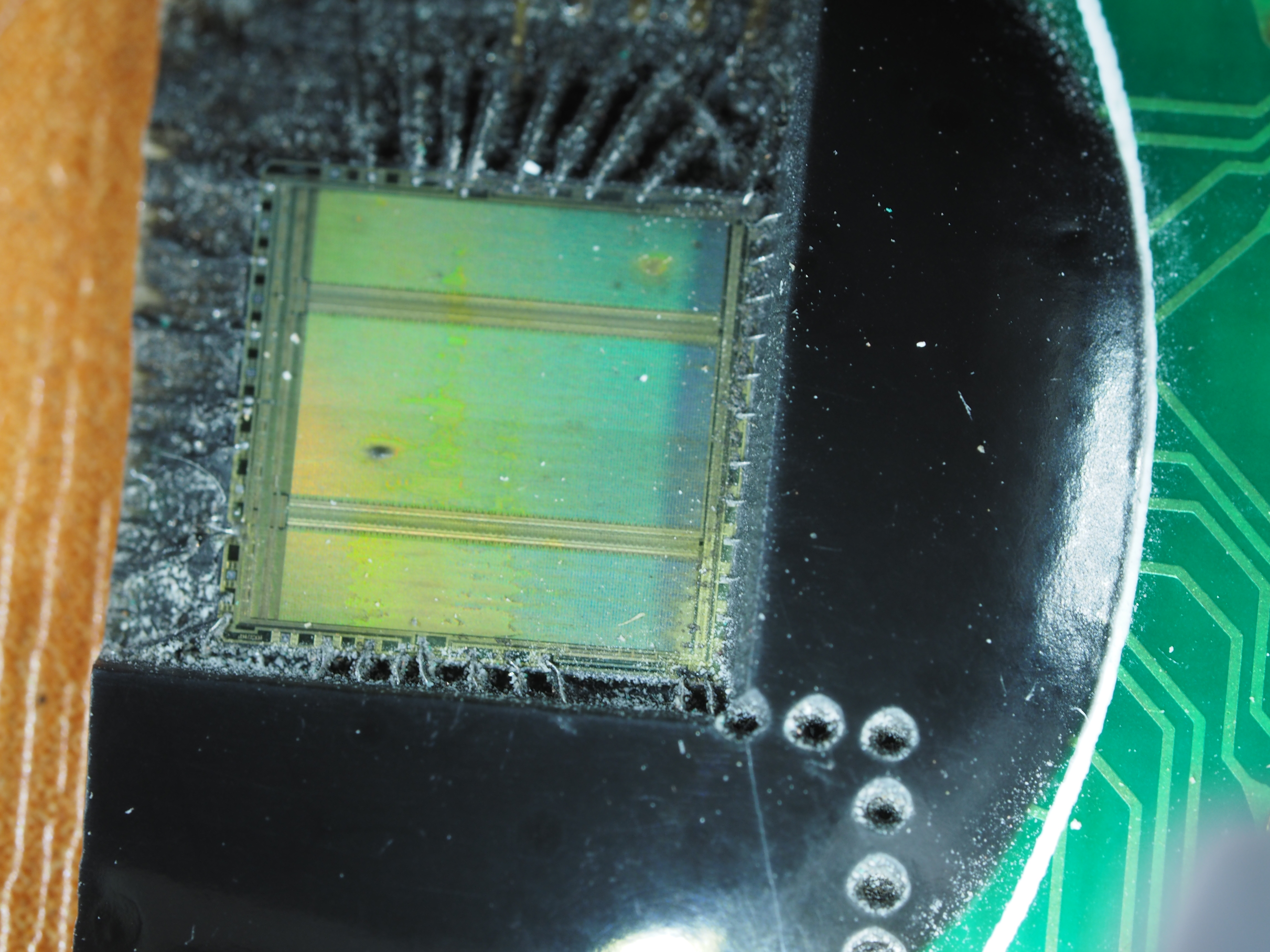
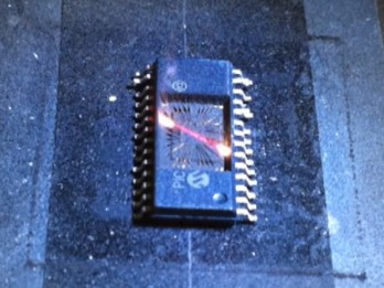
Above: laser decap from below (Source)
https://www.jamiecraig.com/de-encapsulating-ics-with-a-laser-cutter/
- Seemed to work okay
- What would it look like if touched up with WFNA?
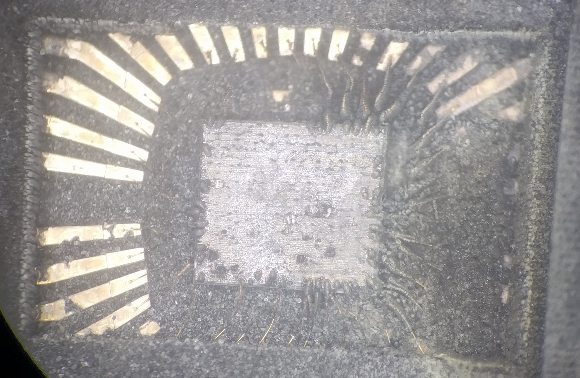
EMSL 6502 test
Silicon Exposed
Above: source
http://siliconexposed.blogspot.com/2013/08/laser-ic-decapsulation-experiments.html
- Poor results
- Cranberry glass
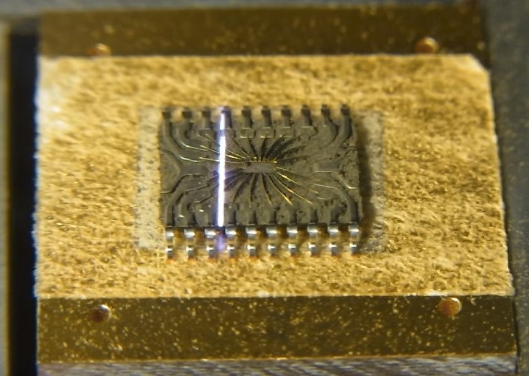
Laser Decap Pro
https://www.youtube.com/watch?v=-x4lyX1C4q0
- Gold backing block
- Good leadframe exposure
- Die unclear how well exposed
- Scanned entire chip (including die area) up until the end
- Raster scan is horizontal, vertical, and diagonal
Sesame 1000
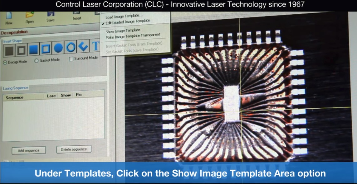
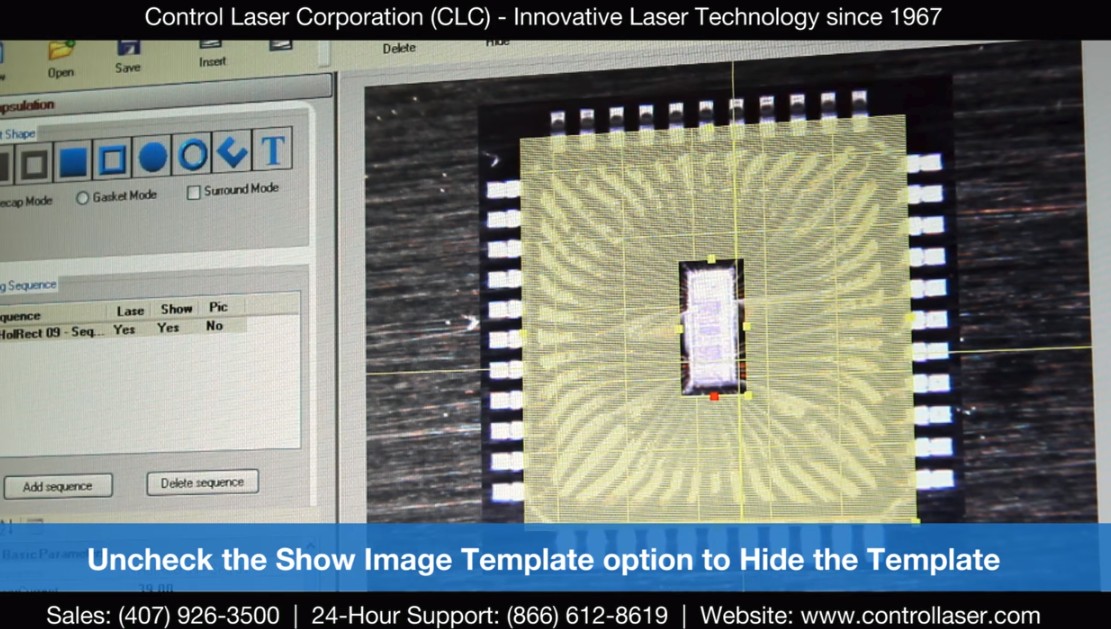
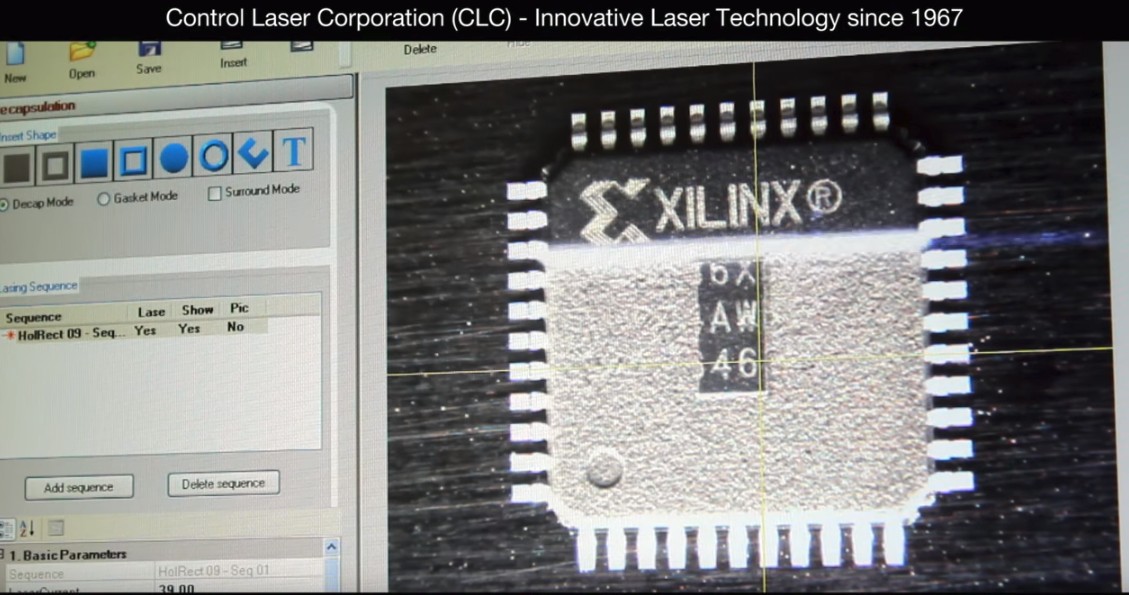
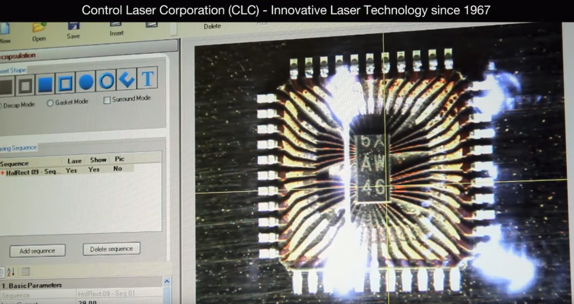
CLC ControlLaser FALIT
https://www.youtube.com/watch?v=SvWgSs2_f00
- Laser Decapsulation FALIT System Software | Image Templates
- Pro system demo
- Has nice features like overlaying x-ray, CSAM, or other guiding image
- Laser scan was horizontal, vertical mix
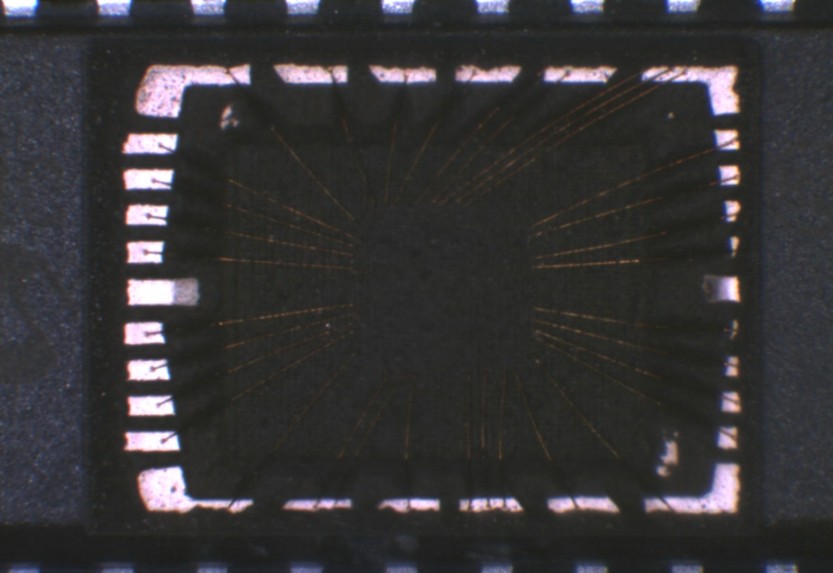
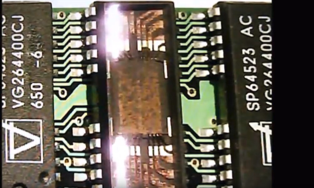
Light Ray
https://www.youtube.com/watch?v=sSRl3Vqbos8
- They do the whole chip but avoid die area
- Light Ray - IC Decapsulation
mcmaster ezlaze
TODO: add pictures, estimate material removal rate
Basically this was too slow to be practical except for very small samples. That said, it did work very well. A quicklase or other higher throughput Nd:YAG system would likely work well
Sandblast
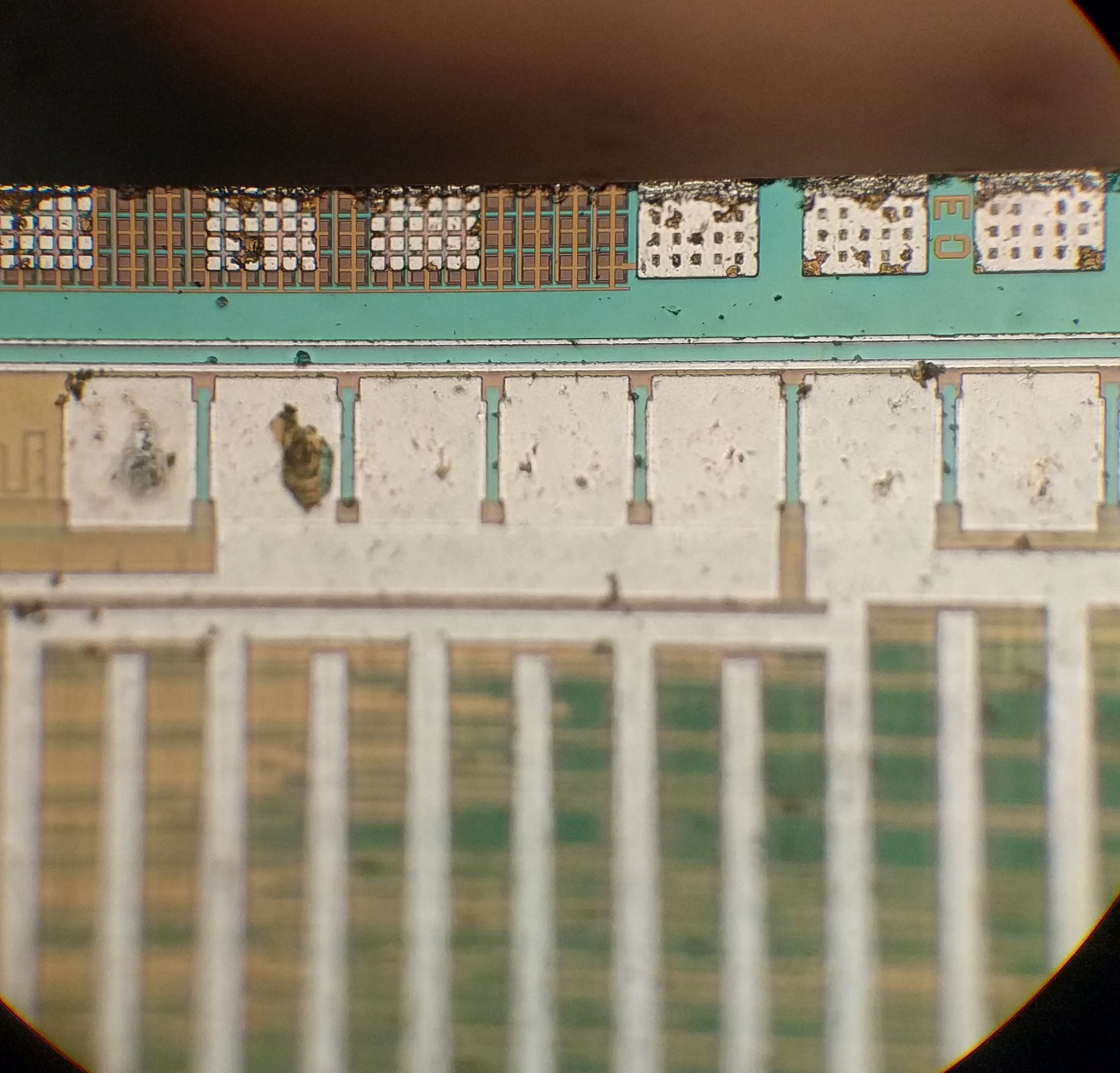
Above: die exposed after blasting with 60 PSI soda. Bond wires have been cleanly removed with minimal surface damage
Price Lynx commercial solution
- Wonder how much surface damage it got?
- Destroyed the bond wires
- Media used?
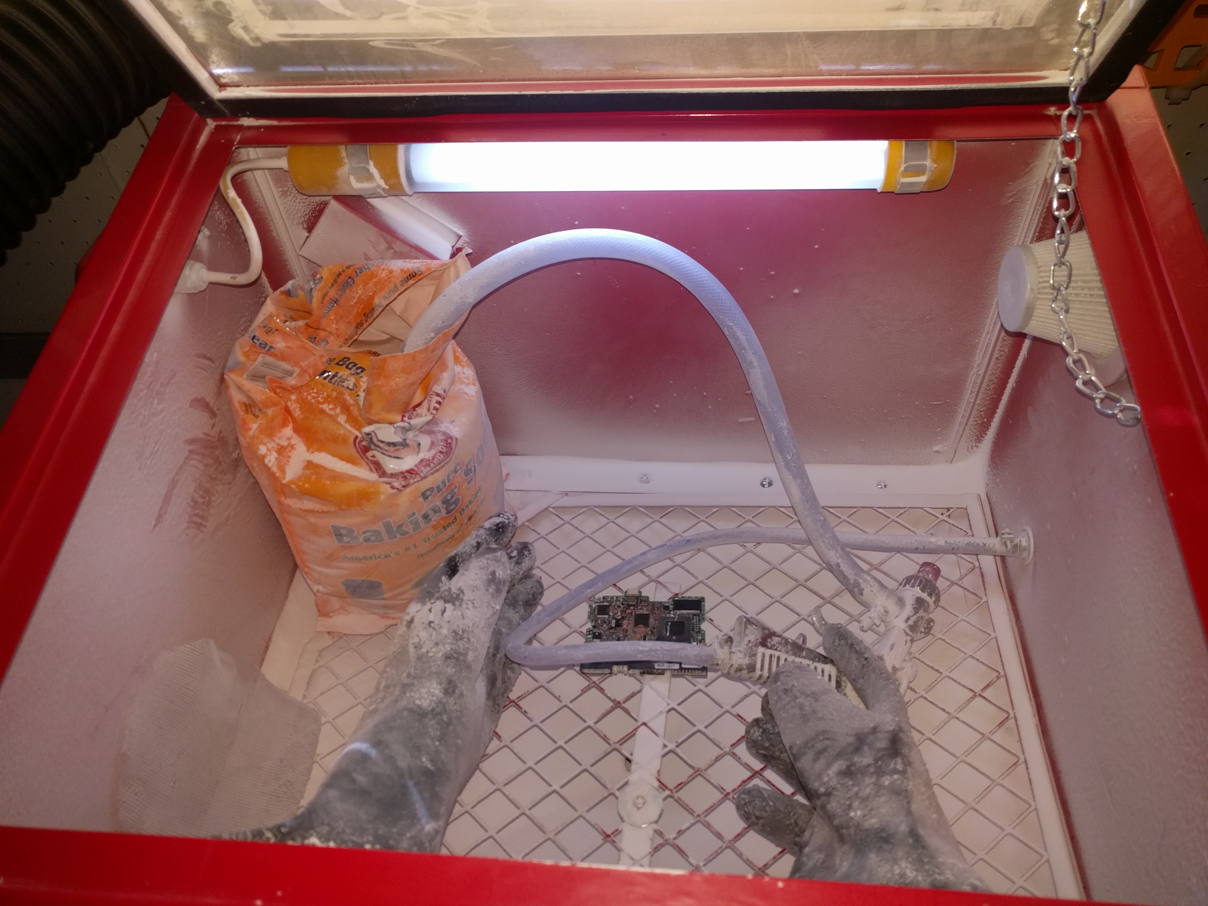
Above: first soda blast test setup
2018-02: mcmaster experiments with baking soda blasting:
- 60 psi at a sharp angle worked okay 2 or 3“ away
- Slow. Consider milling to get near die first
- Destroys bond wires in all tests
- Left reasonably clean bond pads. If sodium ions don't destroy silicon, possibly useful for rebonding
- Main issue I had was actually getting soda to feed reliably
- Blasting at higher pressures definitely caused die damage
- You will need a sizable compressor to run reliably
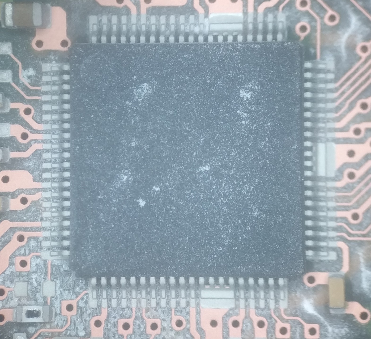
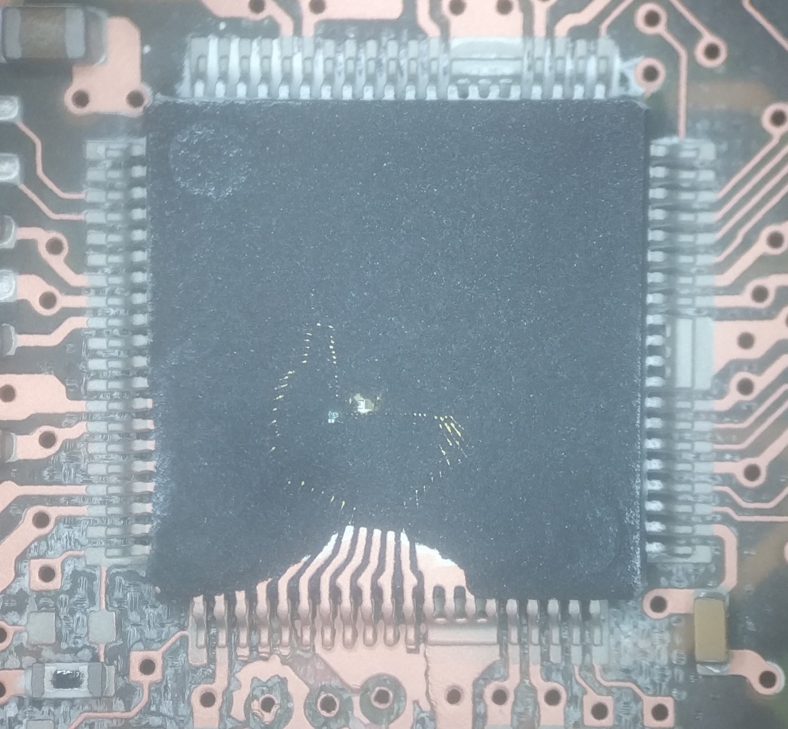
Above: Material getting incrementally removed

Above: tried using metallic tape to protect area from erosion. Tape was quickly destroyed
Epoxy and metal
Some packages contain more than just a simple paddle. Two common examples are:
- Power transistors with large power bus / heat sink
- WDC unusual package
For the most part, use the same techniques that you'd use to remove a paddle from a PDIP
WDC
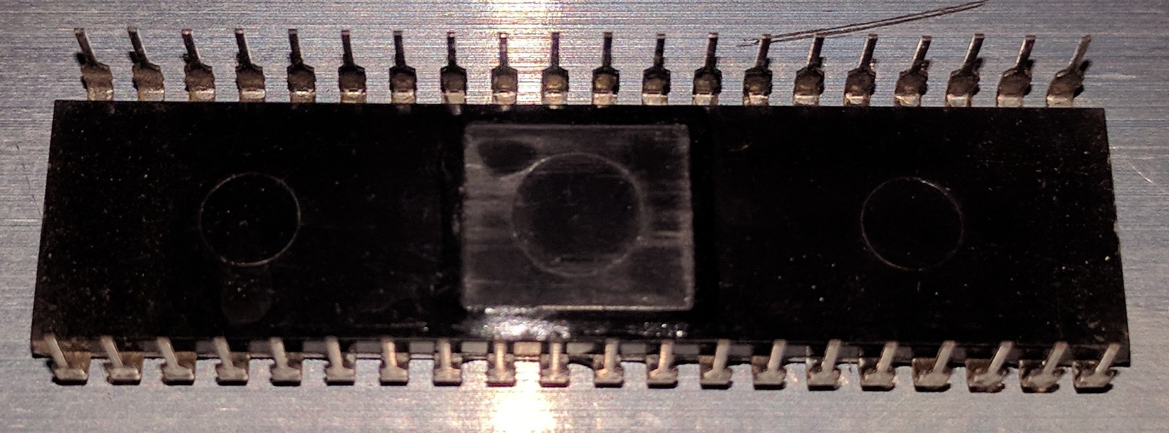
These unusual Western Design Center (WDC) packages are easy to spot with their raised bump on both package sides. Unlike most PDIPs, the die is actually on the bottom of the package, making this a sort of flip chip. Except that the die is still pointed up! The die rests on a metal paddle with epoxy below it.
I tried a few ways to decap these:
- Grind to the metal paddle until release
- Remove epoxy first, then grind down
I found the second to work a little better. To do this:
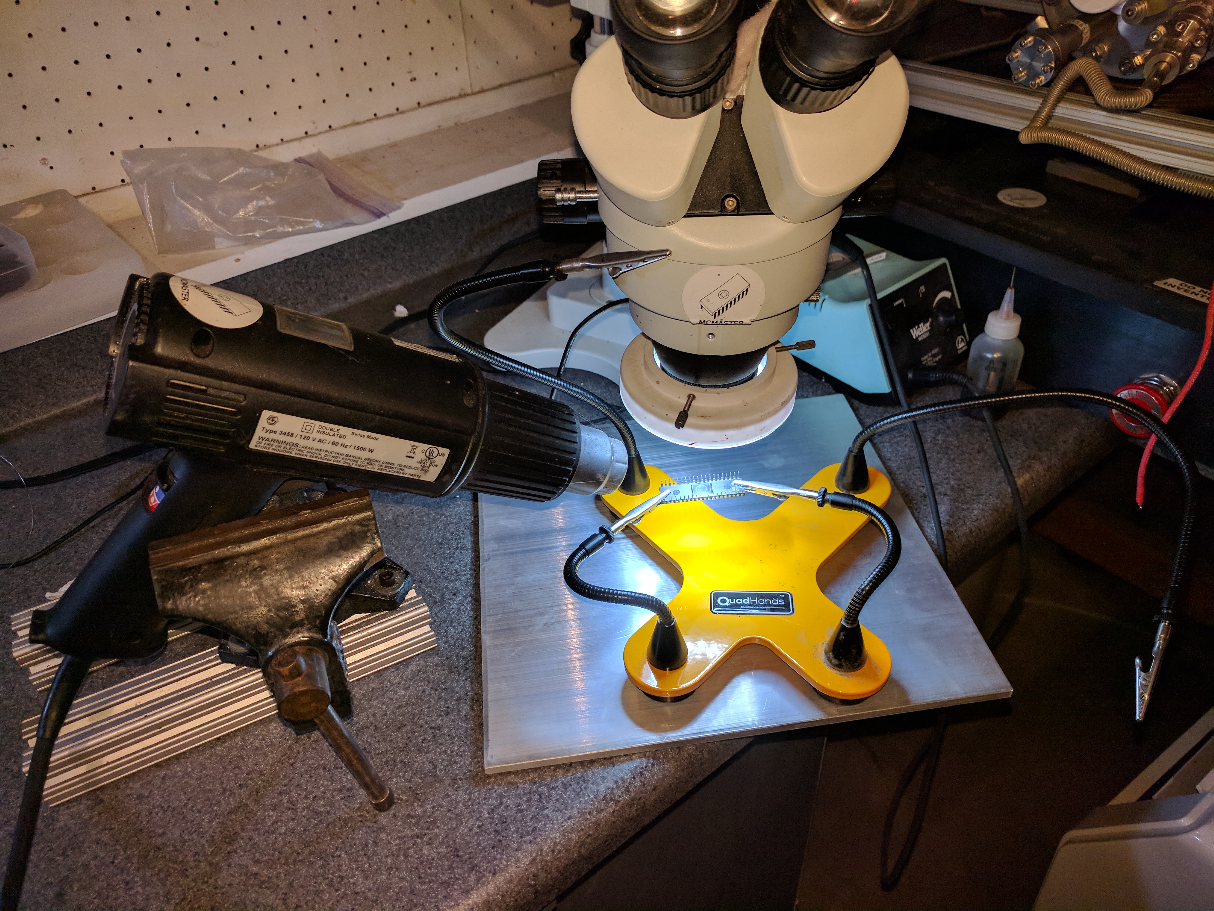
- Mount chip upside down in helping hands
- Turn on heatgun to weaken epoxy
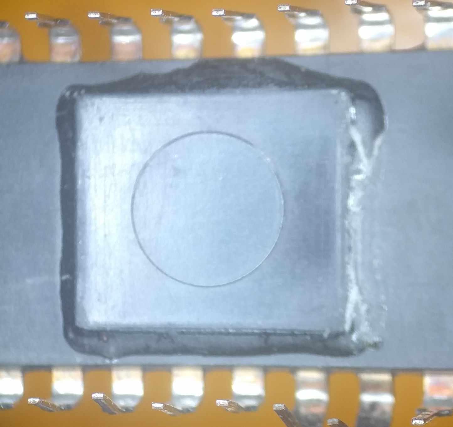
- Use knife to cut around edge, removing sealant
- Pry epoxy cap off by sliding knife under one corner and lifting up
- Gently pry metal paddle out with knife by sliding under one corner
- Turn off heatgun
Following this, re-encapsulate the die with CA glue, placing a kimwipe on it to activate the glue. Then use a relatively weak H2O2/HCl mix to remove the paddle. I used 6 mL HCl with 0.75 mL H2O2, vortexed to help keep it cool. Then soak in acetone to remove most of the glue, followed by a few minutes in hot WFNA to clean it up.
References
- Integrated Circuit Failure Analysis: A Guide to Preparation Techniques
- Abietic acid: http://en.wikipedia.org/wiki/Abietic_acid
- Travis Goodspeed on room temperature decapping using RFNA: http://travisgoodspeed.blogspot.com/2009/06/cold-labless-hno3-decapping-procedure.html
- Sulphuric and other decapsulation: http://www.slideshare.net/mleelcts/decapsulation-process-guide
- Thermomechanical decapsulation: http://www.siliconfareast.com/decap.htm
- Various equipment: http://www3.ntu.edu.sg/home/clgan/mrcfa.htm
- Sulpheric acid decapsulation: http://microblog.routed.net/2008/07/15/how-to-write-an-ic-friday-post/
- Nitric acid gasket compatibility: http://www.efunda.com/designstandards/oring/oring_chemical.cfm?SM=none&SC=Nitric%20Acid


