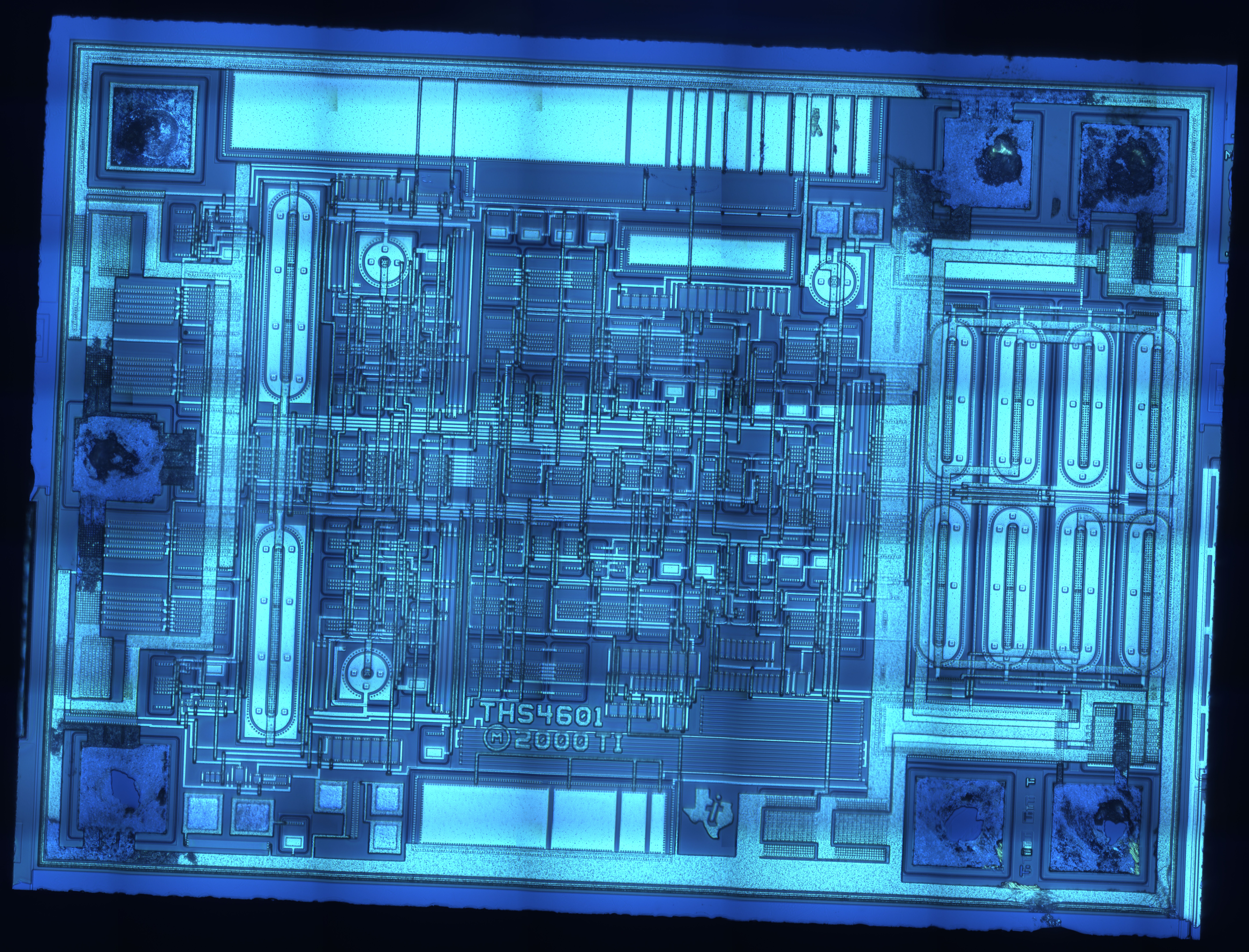
“As promised, I am posting analog circuits yet again. This time we have the THS4601: a wide-band FET-input op-amp. For clarity, I imaged the whole circuit under 400x total magnification resulting in a large file, which is why two 40x objective stitch files are provided. I like this circuit because it makes it possible to have some understanding of the underlying IC schematics. The last image includes labels for the pads and some of the components, so I will refer to these sections in a short discussion. Hopefully these things will make up for the lack of last week’s IC Friday.
The first thing to notice about this chip is, although it has FET inputs, the active load on the input side (right side) is made up of BJTs. This is to improve the bandwidth of the device as BJTs keep providing high effective load values with increasing frequency where a FETs gm might degrade. Furthermore, the connection pattern for the eight devices is such that complementary devices from each input chain are next to each other. This is to keep good load matching in the face of manufacturing differences with the understanding that adjacent devices will more likely undergo the same process as devices at some distance.
Large BJTs are again used to generate a voltage reference, likely to drive a current mirror. The size of these devices is large to, yet again, desensitize the chip to slight manufacturing differences across the die. Over all, this chip uses a fairly large process so any time a metal layer makes electrical contact with a polysilicon layer, a large number of small vias are used. These vias can be viewed as the small pits that litter many of the metal traces. This is done to prevent metal from forming cracks and entering the polysilicon beyond the specified depth due to strain associated with deposition and bonding.”
Source: http://microblog.routed.net/2008/01/04/ic-friday-tis-ths4601/

