Table of Contents
Overview
Map
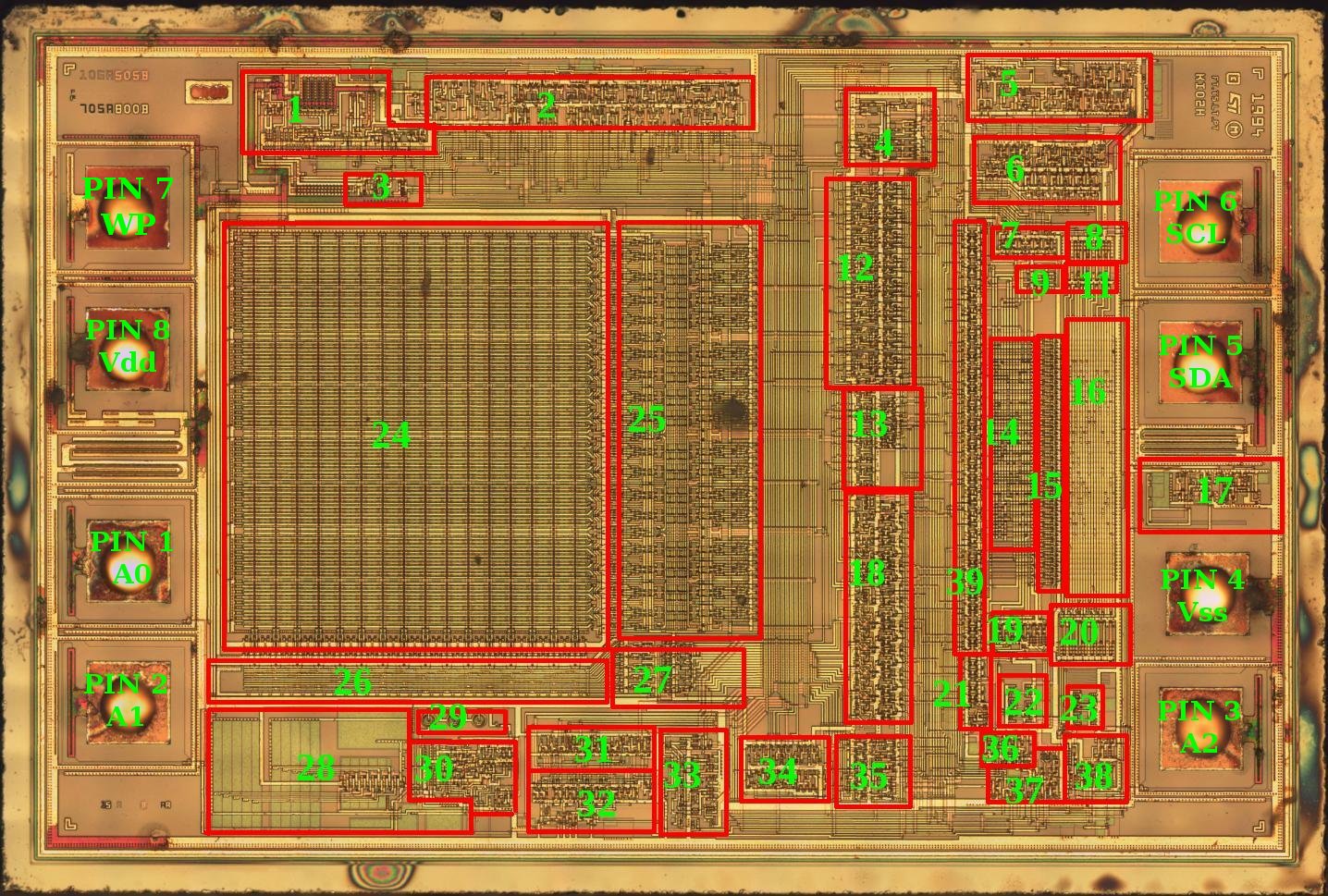
Top metal: https://siliconpr0n.org/map/st/24c02/mcmaster_mz_ns50xu/
Stripped: https://siliconpr0n.org/map/st/24c02/mcmaster_stripped_ns50xu/
Other stuff, just browse around http://siliconpr0n.org/map/st/24c02/
Package
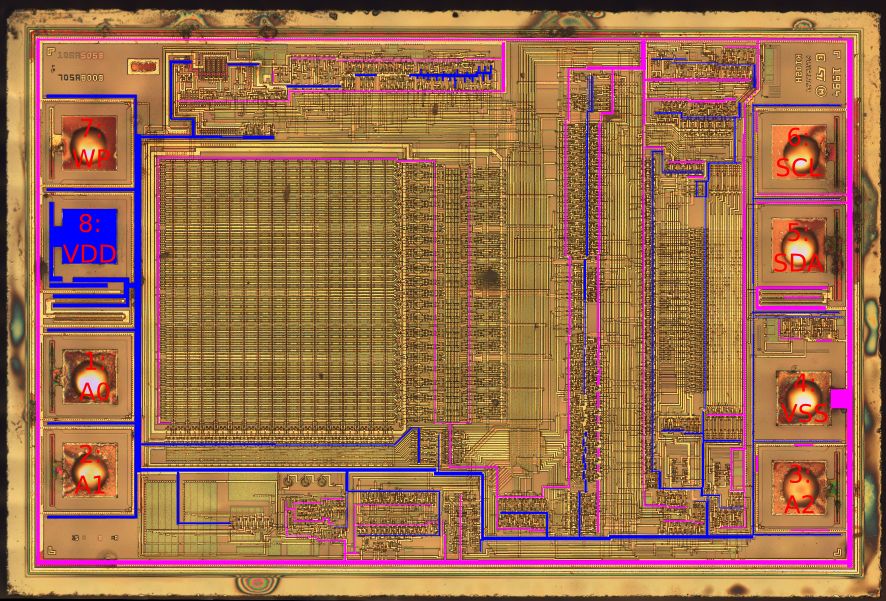
Nets
Sectors
| Number | High level description | Claimed by | Digitized? | Transistor schematic? | Functional schematic? | Other |
|---|---|---|---|---|---|---|
| 1 | Unknown | |||||
| 2 | Unknown | |||||
| 3 | Unknown | |||||
| 4 | Unknown | |||||
| 5 | Unknown | |||||
| 6 | Unknown | |||||
| 7 | Unknown | |||||
| 8 | Unknown | |||||
| 9 | Unknown | |||||
| 10 | Unknown | |||||
| 11 | Unknown | |||||
| 12 | Unknown | |||||
| 13 | Unknown | |||||
| 14 | ROM / microcode? | |||||
| 15 | ROM / microcode? | |||||
| 16 | Unknown | |||||
| 17 | clock? | JM | Y | Y | Half | Right half to meaningful high level schematic. Left half to questionable gate level schematic. |
| 18 | Unknown | |||||
| 19 | Unknown | |||||
| 20 | Unknown | |||||
| 21 | Unknown | |||||
| 22 | Unknown | |||||
| 23 | Unknown | |||||
| 24 | EEPROM | AZ | Y | IP | Still double-checking accuracy of tracing | |
| 25 | EEPROM row/col/data? | |||||
| 26 | EEPROM row/col/data? | |||||
| 27 | EEPROM row/col/data? | |||||
| 28 | charge pump caps and switches | JM | Y | Schematic capture | ||
| 29 | charge pump supply diode? | JM | Y | Schematic capture | ||
| 30 | charge pump control? | JM | Y | Schematic capture | ||
| 31 | Unknown | |||||
| 32 | Unknown | |||||
| 33 | Unknown | |||||
| 34 | Unknown | |||||
| 35 | Unknown | |||||
| 36 | Unknown | |||||
| 37 | Unknown | |||||
| 38 | Unknown | |||||
| 39 | Unknown |
Sector analysis
24 - EEPROM cells
Overview
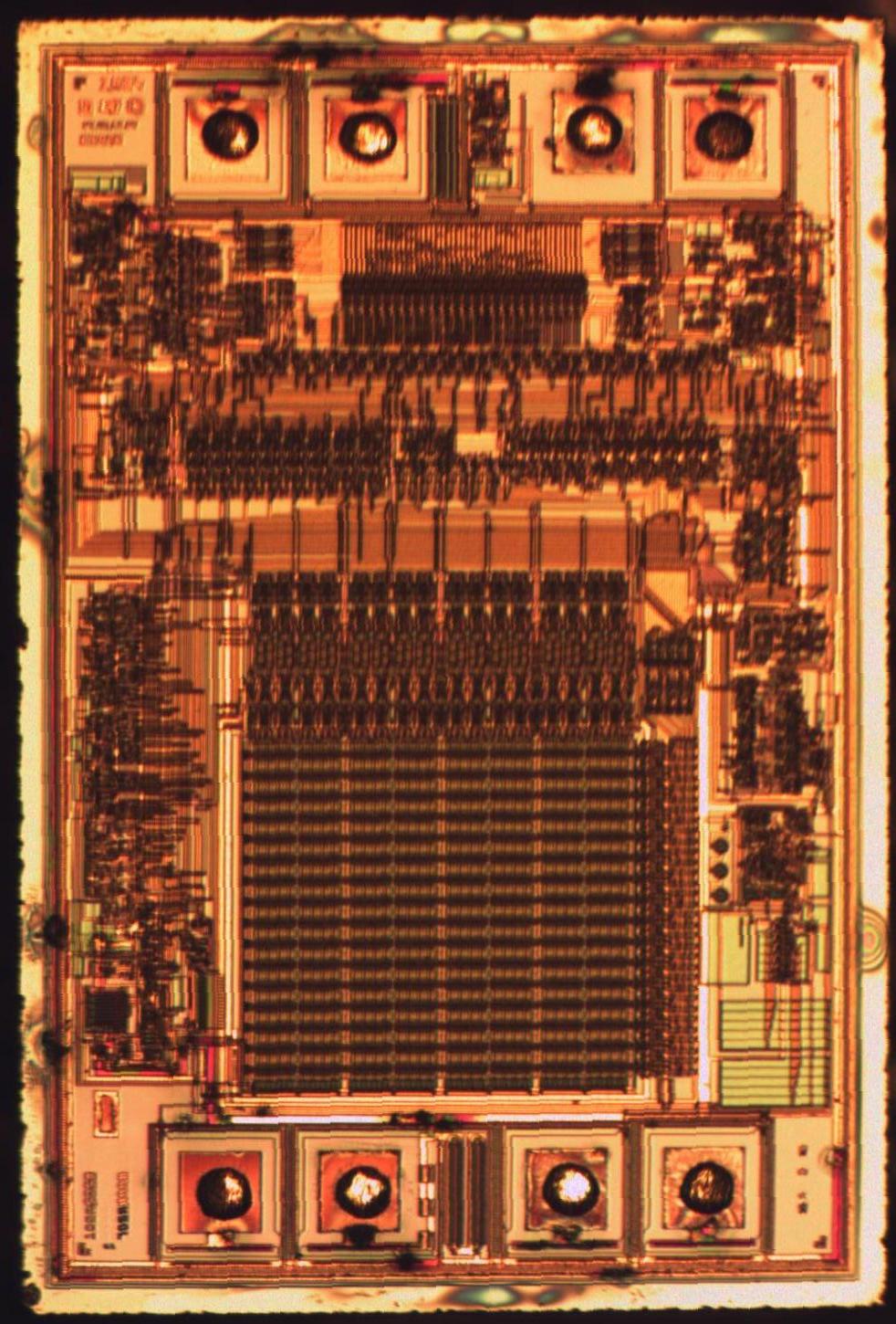
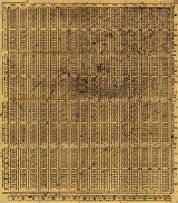
The entire EEPROM array (shown below) is known to be 2048 bits.
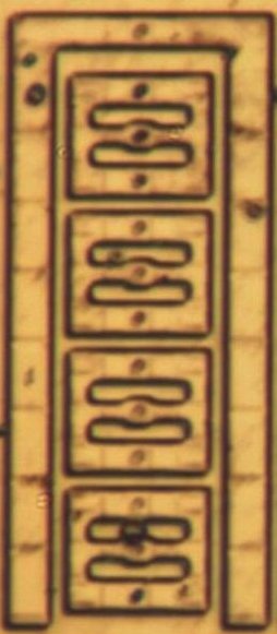
The array consists of a cell (shown below) tiled 16 wide by 8 high, for 128 copies of the cell. Each cell must thus be 16 bits. Each cell consists of four sub-cells, so each sub-cell is 4 bits.
Detailed analysis
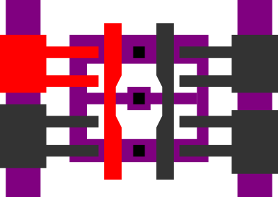
This block contains four EEPROM bits, one per quadrant.
The purple area is active area (doping unknown at this point). The two bars on the left and right appear to be guard rings and can be safely ignored.
Note that each cell contains two horizontal lines (the center is shared) and one vertical.
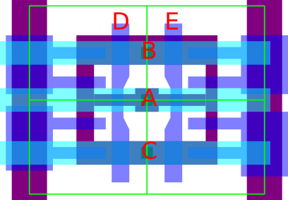
To read out a bit, the column select line for this cell is asserted (active high vs low polarity unknown at this point) and the other deasserted. Suppose we're reading the two bits in the left half.
At this point the left half of the cell (two bits) is active and the right is inactive. Current can now flow between terminals A and B if the upper floating gate is appropriately charged (high vs low unknown at this point) and between A and C if the lower is turned on. In this example the upper left bit is a 1 and the lower left is a 0.
It's not known at this point whether A is driven and B/C are sense lines, or vice versa. The first would allow two bits to be read at a time rather than one but would require twice as many sense amplifiers. If B were driven and A read out, then bit pair “11” would result in C going high which is probably not desirable.
It's also unknown why the floating gates have two fingers over the active area rather than a solid plate. Possibly something to do with leakage? The big plate to the side (over the guard ring) is most likely there to increase capacitance of the floating gate.
The write cycle has not been studied yet.

