Table of Contents
PSoC 4200 series device originally made on Cypress's S8 SONOS process in the Minnesota fab (Fab 4, S8DIN-5R). GSMC in China has also licensed the S8 process technology; traceability markings presumably tell where the device came from but this isn't known yet.
- Cortex-M0 CPU at up to 48 MHz
- 32 KB flash
- 4 KB SRAM
- 36 GPIO pins (4 ports of 8 pins plus one half-port of 4 pins)
- 2 comparators
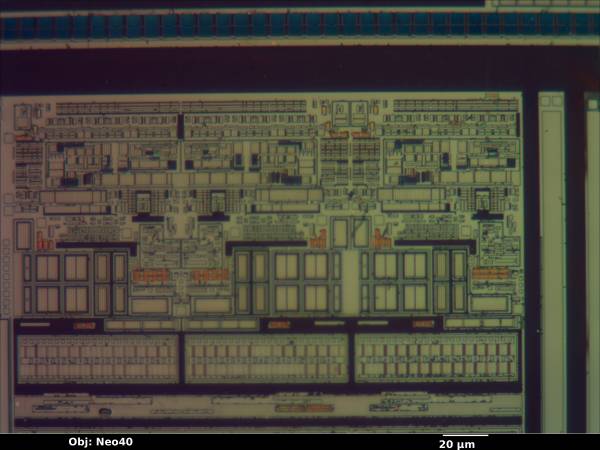
- 4 Universal Digital Blocks (UDBs, basically CPLD function blocks)
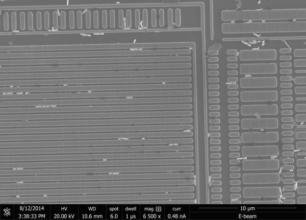
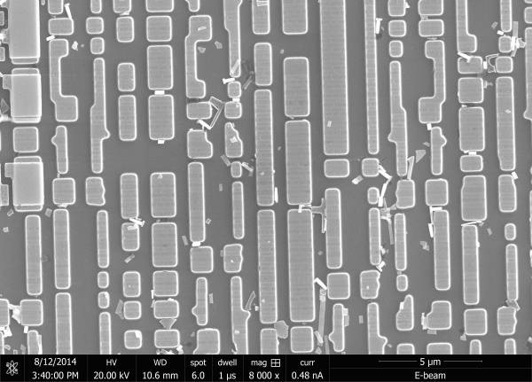
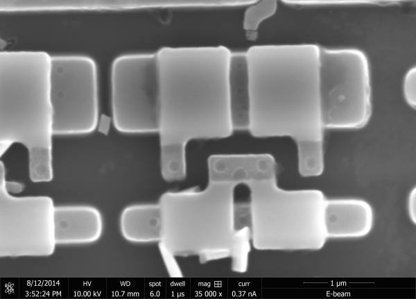
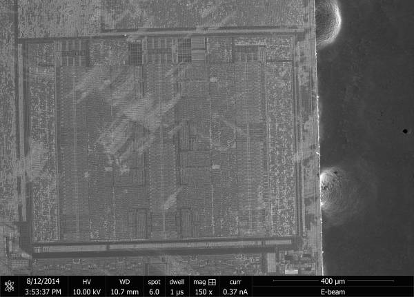
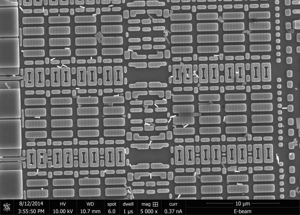
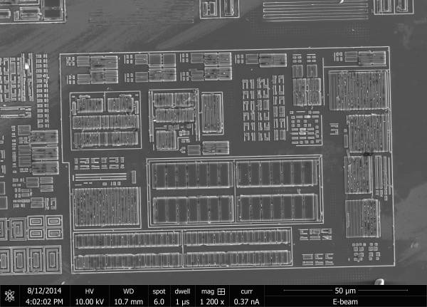
Confirmed by SEM imaging to be 130nm tech, layer count not measured.
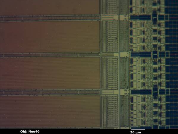
Looks like >= 4 metal layers (thick top metal, at least one vertical-horizontal routing pair, then M1). Full delayering and side-by-side comparison of the UDBs vs CoolRunner-2 architecture is pending.
Stackup from change notice 145273 (TODO: Measure against actual die)
Ti/AlCu/TiW to Ti/TiN/AlCu/Ti/TiN for metallization in fab 4 (except for top layers)
- Metal 1: 150A Ti/250A TiN/3200A Al 0.5% Cu/90A Ti/500A TiN
- Metal 2: 150A Ti/250A TiN/3200A Al 0.5% Cu/90A Ti/500A TiN
- Metal 3: 500A TiW/21,250A Al 0.5% Cu/300A TiW
Passivation: 1000A TEOS/9000A Si3N4
Gate stack: SiO2 / 110A & SiO2 / 32A
Package
Die
Top metal
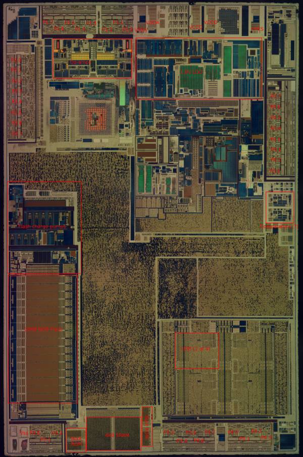
Size is approximately 2120 x 3210 μm (6.80 mm2)
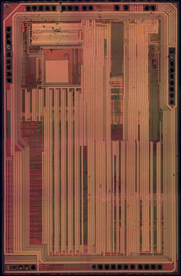
Die overview. Bond pads are mostly grouped into blocks of 9, most likely one ground and eight I/O. The isolated ones in the upper right are probably power, the four at bottom left are probably port 4 since it only has four pins and lacks an associated ground. A full pinout could likely be recovered fairly easily by going clockwise from this block.
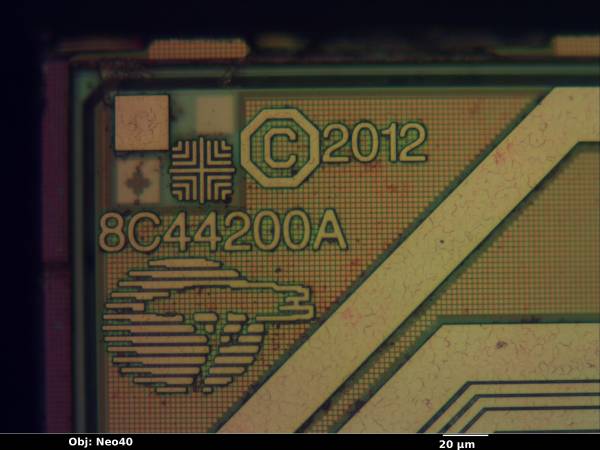
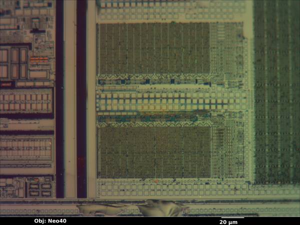
Logo and alignment marks in upper left corner. Note part number “8C44200A” as opposed to the official part number “8C4245AXI”
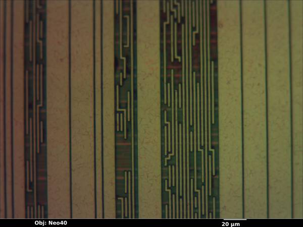
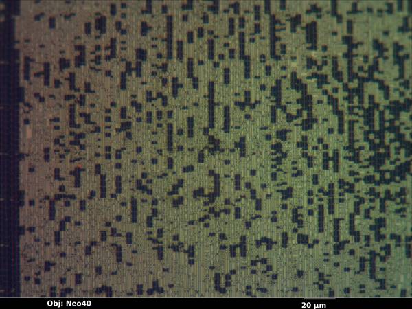
Random vertical interconnect routing on top metal. Smallest observed top metal half-pitch is 1.6 μm (1.7 μm wire, 1.5 μm space). This is very coarse compared to the lower metal layers… either this is a deep-submicron process with thick top metal for power, or they just want low resistance on the top layer for long-range routing of analog signals with minimal losses.
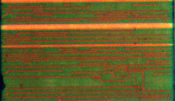
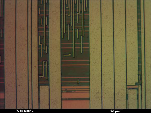
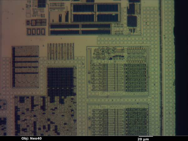
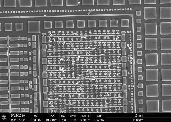
Random horizontal interconnect on Mtop-1. Half-pitch appears to be around 320 nm which is typical x1 pitch for the 180 nm node. Since this is an upper layer the technology node is likely even smaller, perhaps 130 nm. There is at least one vertical routing layer visible below this, and possibly more routing layers before M1 (which isn't visible). Closeup is cropped from full image with contrast boosted.
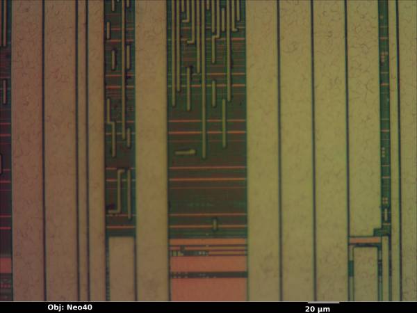
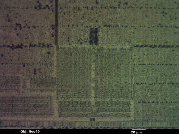
Same region of die with focal plane on Mtop-2.


