This is an old revision of the document!


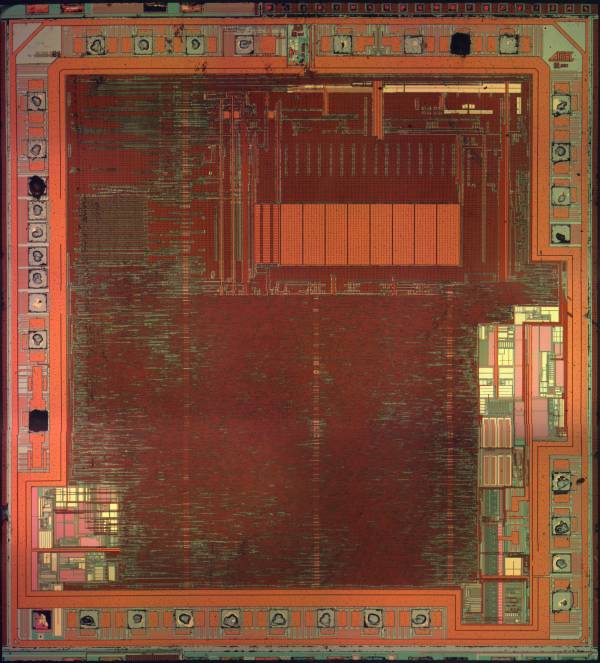
Looks like Atmel's standard 350 nm 3-metal process.

Package markings are weird, looks to be rebranded.

Package

TODO

Die

Dimensions are approximately 2520 μm x 2780 μm (7.01 mm2)

Upper right logo

Top center logo

Top left mask revision markings

Random logic

Some kind of memory

Fuse logic

 
azonenberg/atmel/atmega48.1398558327.txt.gz · Last modified: 2014/04/27 00:25 by azonenberg
 
Except where otherwise noted, content on this wiki is licensed under the following license: CC Attribution 4.0 International
Recent changes RSS feed Donate Powered by PHP Valid XHTML 1.0 Valid CSS Driven by DokuWiki