This is an old revision of the document!
Chips
Processes
| Branded vendor | Branded ID | Process | Die ID |
|---|---|---|---|
Refs:
- Chip IDs on this wiki
CG24 / CG25 gate arrays
B4129AJ Tsutsuji Fujitsu CG24 Cell Library
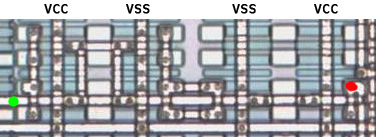
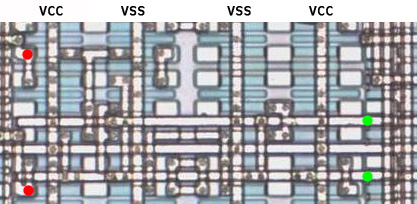
Patent US4661815 describes the architecture and customization method for those chips. They're made of predefined i/o structures framing multiple columns of double CMOS transistor pairs called “Basic cells” (BC), spaced by empty columns for routing.
Customization is done by connecting the transistors with metal to form standard logic cells, which are then connected together and to the i/o structures.
- Red: input to cell.
- Green: output from cell.
All pictures are from 315-5674.
Input pin
Output pin
Bidirectional pin
One trace for input, and two individual traces for the N and P power transistors to allow tri-stating.
Output driver
Bidirectional pin driver
Top input is output level, bottom input is enable. Outputs go to the pin structure transistors. Described page 10 of the MBCG25512 datasheet. Uses 5 BCs.


