Table of Contents
Delayering, also know as deprocessing, are techniques for getting to the various layers in a chip. Typically this is for imaging or microprobing but is also used to alter circuits or to prepare for fault injection. Barring noninvasive methods like CT scan, any delayering procedure will involve removing parts of the chip and will render it permanently non-functional.
Selectively
Main article: Selective removal
Wet etching
Main article: wet
Abrasive
Main article: abrasive
Electrochemical
Main article: electrochemical
Reactive Ion (plasma) Etching (RIE)
Main article: rie
Almost exclusively a professional shop method. Very good results but high barrier to entry ($5000 for a used machine if you're lucky).
Thickness
TODO: get numbers for passivation (SiO2), metal, etc
tox (oxide thickness) scales down with CMOS.
130 nm technology has gate oxides of 20Å or thinner http://en.wikipedia.org/wiki/CMOS
Chemical-Mechanical Planarisation (CMP) considerations
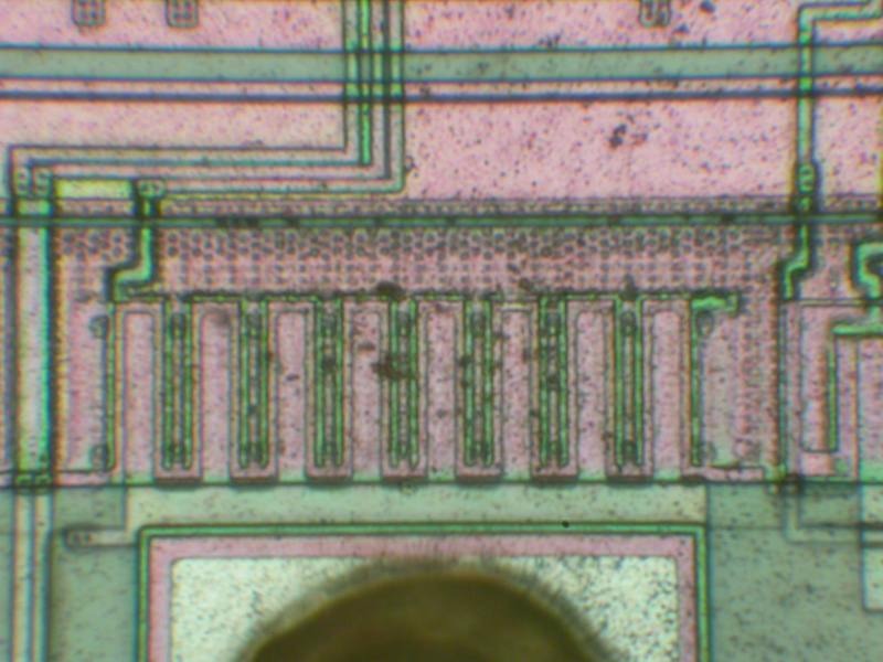
It may not be necessary to delayer depending on the type of analysis being done. For example, 7400 and similar chips often have so few layers and the process technology is so large that a top metal photograph can show transistors.
No CMP:
| Original caption: “Second metal layer and polysilicon layer can be seen through top metal layer on Microchip PIC16F877 microcontroller. 500× magnification.” Copyright 2005 Sergei P. Skorobogatov, used with permission |
CMP:
Lift off
Beck defines “lift off” as “total removal of all layers down to the substrate”. It doesn't seem this is a widely used term but is the only term that we can find for this process. Lift off is important for crystallographic etching. One reason for its lack of popularity might be that the semiconductor field usually refers to lift off as a fabrication technique (see for example http://www.springerlink.com/content/j25g014709338534/#section=85698&page=1).
A. Zonenberg etch rate measurement

Copper etch - 70 ml 3% H2O2 + 10 ml conc. HCl. Heat to 70C, agitate with magnetic stirrer.
Test sample was Altera Stratix IV. Silver or tin plated copper. Plating was gone after <1 min in etchant, metallurgy of the plating was not studied. 20 minutes of etching = 0.13mm removal so 6.5 um/min. This number is likely +/- 30% or so because the temperature of the solution slowly increased over the etch period.
References
- “Semi-invasive attacks - A new approach to hardware security analysis.” Sergei P. Skorobogatov.

