Table of Contents
“Polygon capture” is the process of recovering the original layout and/or schematic based on die images. This is often done as two steps (image ⇒ layout ⇒ schematic) but for quick analysis it may be quicker to generate the schematic directly.
You may run into one of the following scenarios:
- Modern planerized IC
- Traditional non-planerized IC
- Sea of gates (SoG)
- Mask ROM
Modern planarized ICs have regular metal layers and repeated standard cells. This makes the metal easy to capture because it can be snapped to a grid (ie gives error recovery). The metal is also planarized, eliminating artifacts (noise) from other layers to make automated capture easier. Finally, standard cells can be recognized from a pre-tagged list. However, they may require more expensive equipment to image and more involved processes to delayer. They also may also contain a very large number of transistors, forcing automated techniques or more selective analysis.
Non-planerized IC images are generally more difficult to process automatically due to lower layers showing on upper layers. They also are typically full custom designs not using standard cells. However, it may be able to reverse engineer the entire IC from a single image due to the same artifact. This technology also generally limits ICs to simple designs.
Sea of gates use a pre-fabricated active layer that is often metal or contact programmed. This may be non-planarized but will be more regular than a full custom layout.
The general consensus is that planarized chips can be semi-automatically reverse engineered using high contrast images (confocal and/or SEM). However, no-one in the open community has produced a tool that accelerates capturing non-planarized chips. Although metal has proven difficult, I suspect that it would be relatively easy to make a tool to capture the active area of a delayered IC. I have not seen any results for
Mask ROMs are very regular and generally lend themselves well to automated techniques.
See also captured chips
Mask ROM
Note: ROM specific tools are covered on a separate page
Standard cell based
Tools that rely on standard cells or other regular layout
ARES
By Olivier Thomas / Texplained
TODO: youtube presentation Link
Chipworks
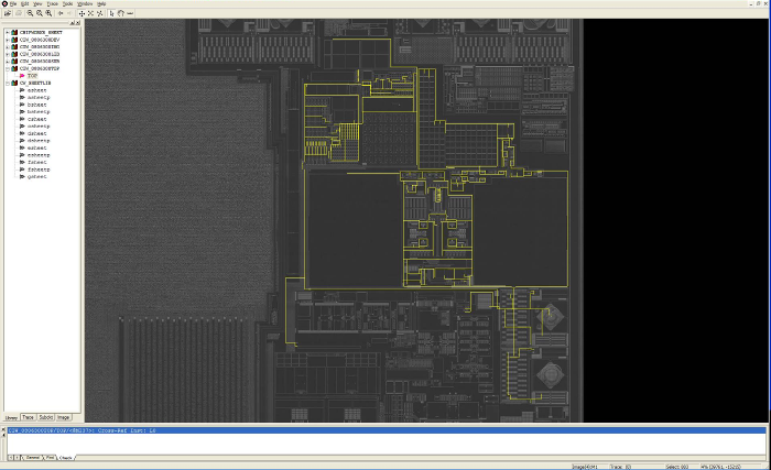
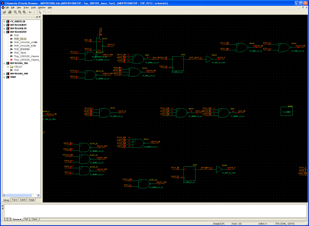
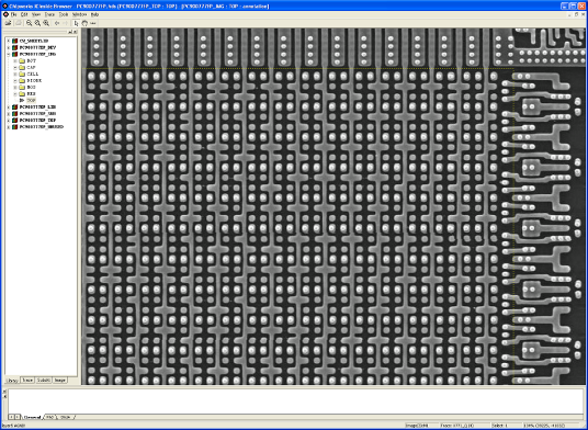
Proprietary internal tool. Some screenshots have been released
As of 2016, I've heard rumors that its analysis capabilities are not very good and its mostly a glorified image viewer with some doodling capabilities. Since I've never used the tool I can't really say
Above: some pictures from http://www.iacr.org/archive/ches2009/57470361/57470361.pdf
Degate
The project
Degate is a multi-platform software for semi-automatic VLSI reverse engineering of digital logic in chips. It is the highest profile FOSS tool, with tutorials and other stuff available.
Little history
Degate was actively developed by Martin Schobert, during his thesis, from 2008 to 2011. For now, the project is inactive and only get some small fixes since 2011. The project is composed of a library (libGate) and a GUI interface (Degate).
In 2016 it was said here:
“Users have noted significant stability issues. I (JM) tried tool again in 2016 and noted considerable stability improvements, but still had it crash on me before I was able to get any results. Still, it might not take that much work to stabilize the tool and unite the community behind it.”
Degate has definitely a great potential, mainly because it is the only free and open-source software for hardware reverse engineering of chips, but never knew how to impose itself in the community. One possible reason for that is because Degate was known to be unstable and have impacting bugs in a first place.
You can visit the initial project website to learn more:
Current status
In 2019, I (Dorian Bachelot) forked the project. This new version aims to totally replace the old Degate, with a focus on Windows and Linux support, getting better stability and general modernization. To achieve this the aim was to drop GTK and move to Qt and merge the lib and the GUI part of the project. Another objective was to minimize the number of dependencies, for now it uses only Boost and Qt and the mid-term objective is to only keep Qt and remove Boost.
The stability was the main problem of the old Degate and the main reason why the community hadn't already united around it. Regarding that, we want to have fewer bugs as possible, even if some functionality needs to be dropped (for the moment).
A lot of bugs were fixed in this newer version, and it should be a better base to improve Degate even more in the future.
Deroute
https://github.com/emu-russia/Deroute
IIRC there was a Degate rewrite. Is this is?
bsim
bitbucket.org/spramod/bsim-tetc14/overview
Implements the following paper algos. Provides aggregation and function inference scheme, but doesn't reach behavioural HDL level.
Flylogic
Known to primarily use photoshop. Focus is on tracing specific (security) circuits rather than trying to capture an entire design
prawnsweeper
An experimental crowdsourced semi-automated polygon capture tool for chips using lambda rules (grid layout)
Above: Playstation 1 CPU top metal test using confocal microscope
psxdev
Non-planerized
Tools that operate on irregular designs
For the most part people use Inkscape, gimp, or photoshop with it mostly being personal preference which tool you use
Automated methods
A number of people have tried but IMHO nobody has beat manual methods yet:
- Robert B: experimented with using neural networks to capture 7400 series chips. Promising, but last I saw needs more testing
- John M: misc tests. Main result was that active layer should be feasible if delayered
- Ken S: tried some things, but think didn't get far
- Visual 6502: don't recall details except that they claimed although they could get some automated, it took more time to fix mistakes than it would to do from scratch
Inkscape
John M
I prefer Inkscape because I've used it for other projects and IMHO a vector drawing program is better suited to the task
General tips:
- Check source images for stitch artifacts before beginning capture
- Gross stitch errors: image misalignment, excessive translation, etc
- Rotation: make sure power buses going around entire chip stay vertical / horizontal
- Consider focusing on a specific area of the chip (IP block)
- Will give you a usable deliverable if you don't finish
- Gives a better sense how everything fits together
- Better sense of time involved
- Consider exploring multiple tools: inkscape, gimp, photoshop
- Especially if you are pretty good with one tool already
TODO
- Find a tool / workflow to morph two separately stitched images into aligned layers
- Crowd source polygon capture
Robert B
He has a pretty cool workflow using a tablet to quickly draw out chips (above link doesn't show this I think)
gimp
IIRC some v6502 folks prefer gimp
Segher
Peter Monta
Visual 6502 tool
Netlist extraction
A lot of people roll their own for this and that
dietools
https://github.com/SiliconAnalysis/dietools
“Series of tools for die shot reverse-engineering”
A few people use this one, so its arguably the most popular
polychip
https://github.com/RobertBaruch/polychip
“Python app to extract a netlist of NMOS transistors from an Inkscape diagram.”
magic
Magic VLSI, along with many other semi tools, should have something of this sort
References
- Reverse Engineering Digital Circuits Using Functional Analysis (Pramod Subramanyan): http://www.academia.edu/2909575/Reverse_Engineering_Digital_Circuits_Using_Functional_Analysis


