Scintillation Detector Applications
using Si Diodes
Detection Technology, Inc.
Micropolis, Finland
In a scintillation-type detector, energy absorbed from incident x-ray, gamma-ray, or charged particles is converted into flashes of light which may be read out by means of a Si photodiode. Depending on the specific application, the signal may be recorded pulse-by-pulse as in very-low-level radiation survey or spectroscopy applications, or integrated (i.e., low-pass-filtered) and read as a current when somewhat higher dose-rates are involved.
There is quite a wide variety of scintillator materials available from manufacturers all over the world. Some suggested vendors are: Bicron, Inc.(1) and Rexon Components, Inc.(2) in the USA; Crystran (3) and Hilger (4) in the U.K.; Scionix (5) in the Netherlands, Unified Technology and Research International (UTARI) in western Canada (6), RAMET (7) in Russia, to name a few.
The choice of which scintillator to use depends on the application -- the energy range and type of radiation to be detected, timing requirements, read-out method, material / fabrication costs, environmental constraints, etc. We have listed a few examples below of scintillator materials which may be used with Si diode read-out. The list is not exhaustive, and the reader is encouraged to consult the scientific literature (8) as well as the scintillator manufacturers' Web sites and technical literature.
Note: The technical data incorporated below is excerpted from material posted on the Bicron, Inc. home page.
SCINTILLATORS
Bismuth Germanate - Bi4Ge3O12
Bismuth Germanate, also called BGO, is a high density scintillation material. Due to the high atomic number of bismuth (83) and its high density, BGO is a very efficient -ray absorber. Because of its high effective Z value, the photofraction for -ray absorption is high, which results in a very good photo-peak to Compton ratio.
The scintillation emission maximum of BGO is centered at 480nm. The scintillation light can be detected with standard photomultiplier tubes. The light yield (photons/MeV- ) is about 20-25% of NaI(Tl), but, since the emission is partly in the region above 500 nm where PM tubes are less sensitive, the relative photocathode yield compared to NaI(Tl) is only ~10-15%.
It also is possible to read out Bismuth Germanate crystals with silicon photo-diodes, but due to the relatively modest light output and less-than optimum spectral characteristic, this is generally only useful in current mode, or for the detection of high energy particles or photons of more than a few MeV in pulse mode.
The scintillation intensity of Bismuth Germanate is a strong function of the temperature. At room temperature, the light output increases approximately 1% for each 1 deg. C drop in temperature. The decay time of BGO is about 300 ns at room temperature, which is comparable to that of NaI(Tl). However, the afterglow is much lower, typically about 0.005% after 3 ms.
BGO scintillation crystals are susceptible to radiation damage starting at radiation doses between 1 and 10 Gray (102 - 103 rad). Since the radiation damage to BGO crystals depends on the presence of sub ppm impurities, large differences between individual crystals can occur.
BGO is relatively hard, rugged, non-hygroscopic crystal which does not cleave. The material does not show any significant self absorption of the scintillation light. The crystal housing can be kept simple since no hermetic air-tight sealing is required. BGO can be machined to various shapes and geometries. BGO scintillation crystals are used in applications where a high photofraction is required (as in PET scanners) or because of its high density (as in Compton suppression spectrometers).
Summary of Properties
Density; 7.13 g/cm3
Cleavage plane -- none
Hardness; 5 Mho
Hygroscopic; no
Wavelength of emission maximum; 480 nm
Lower wavelength cutoff; 320 nm
Refractive index at emission maximum; 2.15
Primary decay time; 300 ns
Afterglow (after 3ms); 0.005 %
Light yield; 8 - 10 x 103 photons/MeV
Photoelectron yield; 15 - 20 % of NaI(Tl) for rays.
Cadmium Tungstate CdWO4
Cadmium tungstate is a high density (7.9 g/cm3), high Z scintillator with a relatively large light yield. The emission maximum is in the region of 500 nm and the total light yield is about 35-40% of NaI(Tl). However, since the emission of CdWO4 is at a much longer wavelength than that of NaI(Tl), the relative photocathode yield is only 25-30% relative to NaI(Tl).
CdWO4 has two emission maxima, one at 470 nm and one at 540 nm. For -ray irradiation, both components are excited. The intensity of the scintillation emission of CdWO4 varies only slightly near room temperature (300 K), which can be important for some applications.
The decay time of the 470 nm component is 20 µs, the 540 nm component has a 5 µs decay time. The afterglow of CdWO4 upon x-ray irradiation is very low, typically less than 0.1% after 3 ms. The material shows a very good radiation resistance: for doses of 104 Gray (106 rad) -rays, the optical transmission of the crystal decreases less than 15%. For -particles, this effect is even smaller: less than 6% for 105 Gray (107 rad).
CdWO4 is a crystal that cleaves very easily and is therefore very susceptible to mechanical and thermal shock. Since some self-absorption of the scintillation light occurs, CdWO4 is usually not fabricated in large dimensions.
Due to the high density of CdWO4, the crystal thickness to
stop 150 keV photons is only 3 mm. The high stopping power and the low
afterglow of CdWO4, together with the possibility to detect the
scintillation light efficiently with photodiodes, make it an attractive
scintillator for x-ray detection (e.g. in CT scanners).
Summary of
Properties
Cleavage Planes (010)
Decay Constant 20.0 µs, 5 µs
Density 7.90 g - cm-3
Emission Spectral Range 330 to 540 nm
Peak Scintillation Wavelength 520 nm
Photons / MeV 13,000
Radiation Length 1.00 cm
Refractive Index at peak emission 2.25
Stability -- Stable (non hygroscopic)
Structure Monoclinic
Cesium Iodide
Cesium iodide has a reasonably high -ray stopping power due to its relatively high density and high effective "Z" (atomic number). For scintillation counting with Si diodes, CsI doped with a thallium "activator" is generally used. This material is designated CsI(Tl).
Cesium iodide has high resistance to thermal and mechanical shock due to the absence of a cleavage plane. Most physical characteristics of CsI are independent of the activator used. Compared to NaI(Tl), CsI is relatively soft and plastic. It is easily fabricated into a variety of detector geometries. Because of its rugged character, Cesium iodide has been extensively used for well logging, space research or other applications where severe shock conditions are encountered.
Cesium iodide itself is soluble in water but is not hygroscopic in the real sense. However, when in contact with materials to which water vapor can adhere, or when used in atmospheres with a high relative humidity, surface degradation can occur. For undoped CsI and CsI(Tl), resurfacing the crystal will generally restore the original performance. CsI(Na) is hygroscopic and must be hermetically sealed at all times just as NaI(Tl).
CsI(Tl) has the highest light output of all presently known scintillators. The maximum of the broad emission is situated at 550 nm and the emission is, therefore, not well matched to a bialkali photocathode photomultiplier tube. This results in a photo-cathode yield for -rays which is only 45% of the value for NaI(Tl). However, the emission spectrum is very well-matched to the sensitivity characteristic of Si PIN diodes, and is often, therefore, the scintillator of choice in such applications.
Summary of Properties
| Scintillator (Activator) | CsI(Tl) | CsI(Na) | CsI(undoped) |
| Density [g/cm3 | 4.51 | 4.51 | 4.51 |
| Hygroscopic | slightly | yes | slightly |
| Emission wavelength max [nm] | 550 | 420 | 315 |
| Lower Cut-off [nm] | 320 | 300 | 260 |
| Refractive index @ emission max | 1.79 | 1.84 | 1.95 |
| Primary decay time [µsec] | 1.0 | 0.63 | 0.016 |
| Light yield [photons/MeV ] | 52- 56 x103 | 38-44x103 | 2x10³ |
| PMT Photocathode yield [% of NaI(Tl)] | 45% | 85% | 4% - 6% |
Converting gamma -ray energy to electronic charge
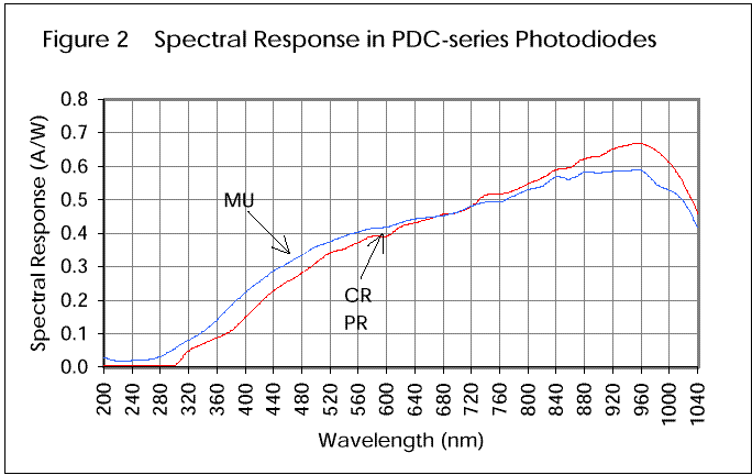
Quantum Efficiency for a photo-diode is the number of electron - hole pairs that can be detected as a photo-current divided by the number of incident photons. This is usually expressed as a "percent" (at a particular wavelength) and is given by the following relationship:
QE(lambda) = S(lambda) ÷ (lambda) x 1240 x 100%
Where S is the photo sensitivity in A/W at a particular wavelength, and (lambda) is the wavelength expressed in nm (nanometers).
Example 1: From Fig. 2 above, the quantum efficiency of a PDC-series diode with a resin window coupled to a CsI(Tl) scintillation crystal whose spectral peak is centered at 550 nanometers is the spectral sensitivity at 550 nm (~0.37 A/W) ÷ 550 x 1240 or ~83%.
Pulse Mode readout using CsI(Tl)
Choice of Diode: In general, pulse-mode read-out requires the use of a back-biased PIN type of photodiode (PDC series) which has a much lower junction capacitance for a given active area, and consequently a much faster signal response, compared with that of a planar photo-diode (PDA series) of the same active area.
Optical Coupling: Since the index of refraction of most scintillation crystals is substantially higher than 1.0 (1.0 is the index for air and is close to the value for the resin window on a Si diode), getting the scintillation light out of the crystal and into the diode almost always requires the use of an optical coupling medium - a gel or silicone grease for temporary construction, or an epoxy-based compound or other resin-type adhesive for permanent construction.
For optimum light-transmission, the coupling medium should have an index of refraction which is the geometric mean (i.e., the square root of the product) of the indices for the crystal and the entrance window of the diode.
Determining the efficiency of optical coupling in a scintillation detector: One can estimate the optical coupling efficiency between crystal and photodiode using a small (~1 uCi) low-energy gamma-emitting check-source, such as 241Am (59.5 KeV principal gamma emission). This is about the maximum useful energy for this technique, since detection efficiency in a Si photodiode drops very quickly at higher photon energies, and detection in the scintillator crystal begins to swamp the the overall system count-rate.
Assuming the detector assembly is not completely opaque to the 59.5 KeV gamma rays, one can position the source on the rear (diode side) of the detector so that some of the incident radiation is detected directly in the PIN photodiode, rather than in the crystal. The results of one such experiment are shown below. The detection efficiency for 59.5 KeV gamma rays in Si is rather low (~1%), and the attenuation of 59.5 KeV gamma rays by the detector assembly itself is rather high, so these measurements took a few hours to acquire.
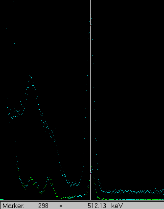
In the figure above, the top-most spectrum is from a 22Na source detected in a 1 cm3 CsI(Tl) scintillating crystal coupled to a 1 cm2 Si PIN diode. The prominent peak is at 511 KeV. The lower spectrum shows a partial gamma ray spectrum from 241 Am detected directly in the Si photodiode, where all of the system parameters, gains, etc., are unchanged from one measurement to the next.
The 511 KeV peak in CsI(Tl) corresponds to channel 297; the 59.5 KeV peak in Si corresponds to channel 302. We know from our data on CsI(Tl) that the conversion from gamma ray energy to optical photons is ~55,000 photons per (absorbed) MeV, or 28,105 photons at 511 KeV. We also know that it requires 3.6 eV to produce one charge-pair (electron-hole pair) for direct detection in Si. Based on the latter measurement we have an absolute measure of electronic charge versus channel number: 59.5 KeV corresponds to 59,500 ÷3.6 = 16,528 electron-hole pairs, or 2.644 x 10⁻¹⁵ coulombs which, in turn, corresponds to channel 302.
The peak at channel 297 from 511 KeV in CsI(Tl) corresponds to a slightly lower value -- 2.6 x 10⁻¹⁵ coulombs. We started with 28,105 optical photons, and the quantum efficiency of our photodiode is ~83%, so if the optical coupling efficiency were perfect we would expect an electronic pulse of 0.83 x 28,105 = 23,327 charge-pairs, or 3.73 x 10⁻¹⁵ coulombs.
However, our 511 KeV scintillation peak turns out to be only ~70% of this value, so we must conclude that the overall optical coupling efficiency for this detector is only ~70%, leaving some room for improvement.
Example 2: Estimate the amount of electronic charge generated in a Si PIN diode from a scintillation flash produced by a 140 KeV gamma-ray photon which is fully absorbed in the CsI(Tl) crystal scintillation detector discussed above.
From the "summary of properties" chart for CsI(Tl) we know that 140 KeV of gamma-ray energy absorbed in CsI(Tl) produces ~55,000 light photons - MeV-1 x 0.14 MeV = 7700 photons. Assume 70% optical coupling efficiency into our Si diode. From Example 1 above, our diode has ~83% quantum efficiency at 550 nm, so the amount of charge contained in the Photo-diode signal pulse from a 140 KeV scintillation event in CsI(Tl) is ~0.83 x 7700 x 0.7 = 4473 electron-hole pairs, or ~7.15 x 10⁻¹⁶ coulombs.
This is a very small signal indeed: Precision is limited to a large extent - particularly at room temperature and higher - by electronic noise due to diode leakage current and amplifier "front-end" noise. The noise floor for a 1 cm2 PIN diode, such as the DTI type PDC-100S, optimally matched to a 1 cm3CsI(Tl) crystal, is approximately 40 KeV. Care and considerable technique is required to achieve the best in low-noise performance in pulse-mode spectroscopy and similar applications using scintillators coupled to photodiodes.
Pulse-mode amplification of such weak signals is best implemented using a charge-integrating preamplifier (9) which is configured for the specific type of Si diode being used. In particular, for optimum noise performance, the preamplifier input stage should be a low-noise junction-type field-effect transistor (JFET) whose input capacitance matches (nominally) the photo-diode junction capacitance.
In addition, for best noise performance, the shaping time constant of the following stage(s) of amplification must be long enough to encompass the entire scintillation pulse. Many scintillators (see summaries of characteristics listed above) have more than one time constant in their emission decay characteristic. However, the listings often specify only the dominant, or in some cases, an "effective" or "average" decay time which does not necessarily incorporate some of the slower components.
However, these slower components may contain several percent or more of the total scintillation light. Where the highest measurement precision is required, adequate integration, or shaping time, must be provided. In the case of CsI(Tl), for example, shaping times in excess of 6-8 µseconds are required to convert all of the light into electronic charge.
Scintillation Broadening
The pulse-height resolution in CsI(Tl) is further degraded by a Scintillation broadening phenomenon (10) presumably related to inhomogeneity in the volume distribution of the Tl activator within the crystal . This effect is clearly visible in the figure above, in which the position of the centroid of the 511 KeV peak in CsI(Tl) is nominally the same as that for direct detection of 59.5 KeV gamma rays in Si, but for the same (average) electronic pulse amplitude, the width of the 511 KeV peak in CsI(Tl) is approximately twice that of the corresponding peak for direct-detection of 59.5 gamma rays; i.e., the pulse-width in CsI(Tl) is much broader than would be expected from a consideration of electronic noise and photon statistics only.
Current Mode read-out
Current mode measurements on Scintillation-type detectors may employ either planar Si diodes (PDA series) or PIN Si photodiodes (PDC series). Depending on the particular application, both types may be operated with or without back-bias. In either case, unbiased operation is generally preferred when the lowest possible leakage current is required.
The junction capacitance is much lower (and the signal response becomes correspondingly faster) when a back-bias is applied. For a given area (and back-bias), the planar photo-diode offers substantially lower leakage current, but with a very much higher junction capacitance producing, in turn, a slower signal response relative to the PIN device. Quantitative comparison and evaluation of the various trade-offs associated with choice of a particular diode type and operating mode requires a careful examination of the respective DTI device data sheets.
Current mode read-out almost always employs a trans-resistance (current-to-voltage converter) type of amplifier. The photo-diode is connected to the inverting input terminal of a high-quality operational amplifier with resistive feedback. The trans-resistance gain, expressed in ohms, is simply the value of the feedback resistor. Trans-resistance gains of tens, hundreds, or even thousands of megohms are commonly utilized in low-level radiation detection applications.
For additional information regarding the design and implementation of high-performance trans-resistance amplifiers, see the Application Note entitled An Ultra-Low Level Light - or Radiation-Sensor from Detection Technology, Inc.
REFERENCES
4. http://www.hilger-crystals.co.uk
5. http://www.scionixusa.com/scintillation_detectors.html
7. http://www.girmet.ru/~ramet/scintillator.htm
8. An exceptionally rich source of up-to-date reference material on scintillators and Si diode read-out is the "publications" Web Page, University of California, Lawrence Berkeley National Laboratories, Center for Functional Imaging http://cfi.lbl.gov/instrumentation/Publications.html
9. Chapter 17 in Radiation Detection and Measurement by G.F. Knoll; John Wiley & Sons, publishers; ISBN 0-471-49545-X
10. I. Holl, et al, "A Measurement of the Light Yield of some Common Inorganic Scintillators" in Selected Papers on Phosphors, Light-Emitting Diodes, and Scintillators. Marvin J. Wheeler, Ed. SPIE Milestone Series, Volume MS151. International Society for Optical Engineering, Bellingham, Wa, USA, 1998. ISBN 0-8194-2977. An abridged version of this paper is published in IEEE Trans on Nucl Science, Vol. 35(1), pp. 105-109 (1988).