Home
Output Circuit Values & MOSFET ratings
High Power & Harmonic Reduction
Construction Overview
Simple 400 Watt
RF Amp for
80 meters
Pulse Width Modulator and power supply
Analog Modulator (Class H) and power supply
![]()
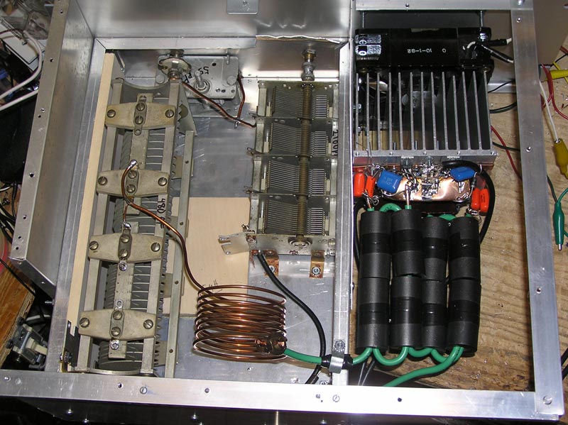
The Two Module, 400 Watt RF Amplifier 80 Meters
Click here for the schematic in PDF format
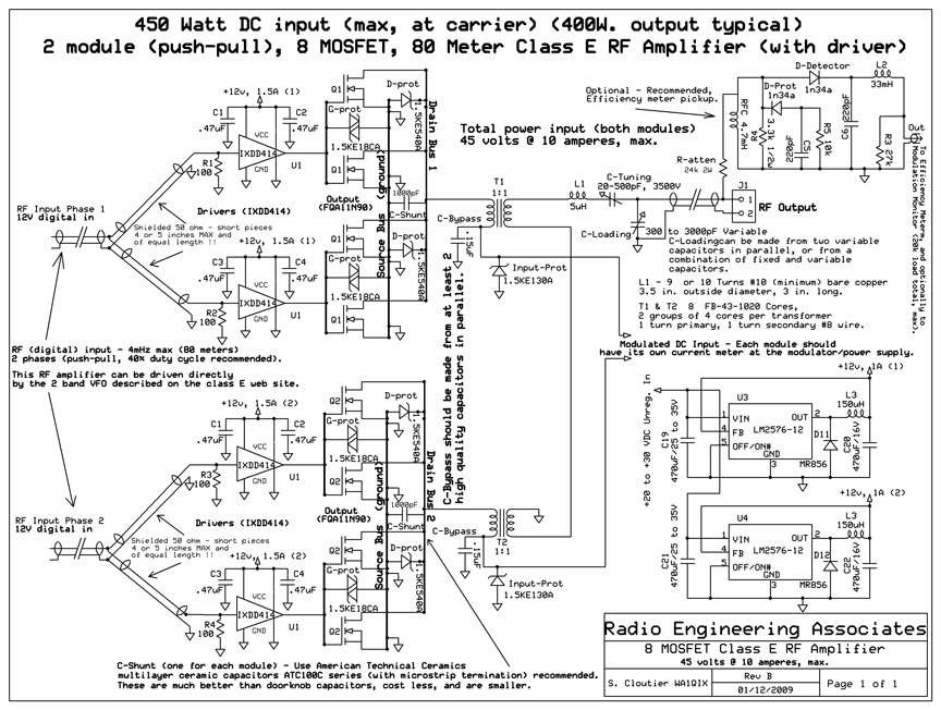
The 8 MOSFET RF amplifier consists of two identical 4 MOSFET RF amplifier stages connected together in a single ended push pull configuration. Each amplifier stage (module) includes an RF driver (IXDD414 ICs), one IC for every 2 MOSFETs. The driver IC inputs are connected together to form a semi "bus", with a 100 ohm termination resistor connected to ground at each end of the driver bus, forming a 50 ohm termination. The drivers are connected to the VFO using 50 ohm coaxial cable.
Each driver bus is driven out of phase with the other, so when one is "on" the other is "off". The outputs are also combined out of phase, giving the single ended, push pull configuration. TVS (TransZorb) devices are used on the drain and gate busses, and on the modulated DC input to each amplifier stage.
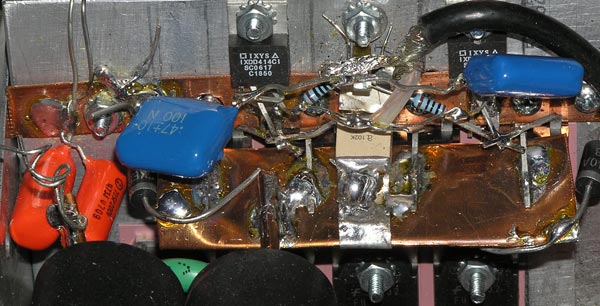
Construction Notes: The shunt capacitors C-Shunt in the schematic are ATC (American Technical Ceramics) ATC100C series capacitors, 1000pF, 20% with MicroStrip (MS) termination. The MicroStrips are made from solid silver, and make it very easy to install and solder the capacitors into the circuit.
The .15uF RF bypass capacitors (C-Bypass) are made from 2 orange drop capacitors in parallel. 2 or 3 capacitors may be used in combination to obtain the desired capacitance value. The capacitors should by high current, low ESR (series reactance-resistance) good quality capacitors.
Note: The exact value of the RF bypass capacitors is not critical. Anything between .12 and .17 uF will work very well. If you are using a pulse width modulator, the RF bypass capacitor becomes part of the last capacitor in the PWM filter, and the value of the bypass capacitor must be known when building the filter.
Driver
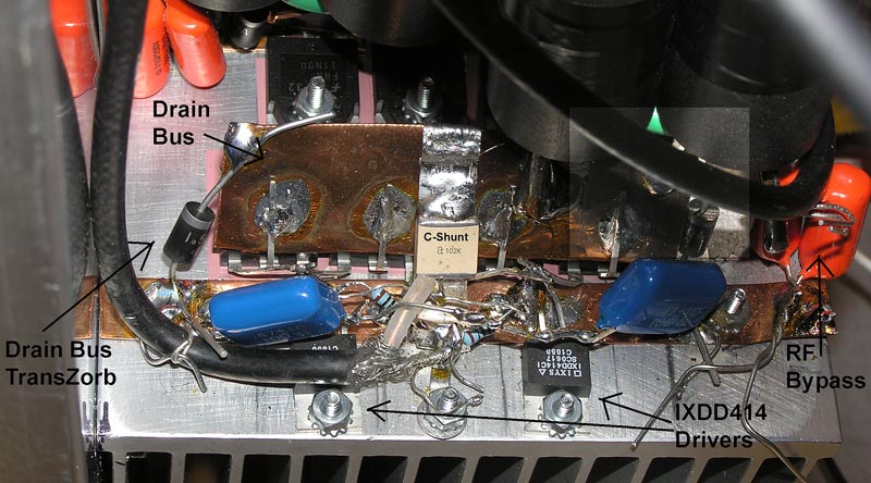 The transmitter uses IXDD414 driver ICs, one for every 2 MOSFETs (on 75 meters).
Each driver IC has its own RF bypass capacitor, connected from the VCC to
the ground plane. The power requirement for the driver ICs on 75 meters
(all 4 drivers) is around 2.5 amperes at 12VDC.
An LM2576, pulse width modulator IC can deliver up to 3 amperes of DC at 12V
- more than enough current for the 4 IXDD414s on 75 meters.
The transmitter uses IXDD414 driver ICs, one for every 2 MOSFETs (on 75 meters).
Each driver IC has its own RF bypass capacitor, connected from the VCC to
the ground plane. The power requirement for the driver ICs on 75 meters
(all 4 drivers) is around 2.5 amperes at 12VDC.
An LM2576, pulse width modulator IC can deliver up to 3 amperes of DC at 12V
- more than enough current for the 4 IXDD414s on 75 meters.
The output terminal of each of the driver ICs is connected directly to the gates
of 2 of the FQA11N90 output MOSFETs. In this particular example, the gate
leads of the FQA11N90s are bent in such a way as to faciliate a direct connection,
and the output of the IXDD414 is connected to the junction of the gate leads.
A small bus can also be used.
 The ground terminals of
each driver ICs are connected directly to the source bus, and the tab (also
ground for the driver ICs) is bolted directly to the heat sink. All
interconnecting leads should be kept as short as possible to minimize stray
inductance, particularly the driver RF bypass capacitor connections.
The ground terminals of
each driver ICs are connected directly to the source bus, and the tab (also
ground for the driver ICs) is bolted directly to the heat sink. All
interconnecting leads should be kept as short as possible to minimize stray
inductance, particularly the driver RF bypass capacitor connections.
The input to the drivers is delivered via 50 ohm coax cable (RG58 or similar 50 ohm thin cable), and each cable is terminated by a 2 100 ohm resistors, one at each IXDD414 driver IC (2 driver ICs per module), forming a 50 ohm termination.
The gate waveform produced by a single IXDD414 driver driving
2 FQA11N90 MOSFETs is
very good on 75 meters, and approaches
a true square wave on 160 meters. This results
in a very stable and efficient class E amplifier.

RF Output Transformers
This 2 module class E RF amplifier uses 2 RF output transformers, one for each module. The RF output transformers are each construted using 8 FB-43-1020 (type 43) cores, stacked in 2 groups of 4 cores each, 8 cores per transformer. The primary and secondary windings consist of a single loop of #8 solid copper, insulated wire.The primaries consist of a single U shaped loop of wire, and the secondaries consist of a similar U shaped loop, running in the opposite direction. The 2 secondaries are constructed using a single run of wire, running between the 2 transformers, however there is no reason why the secondaries could not be constructed from individual U shaped pieces, connected together using split bolts.
The primary windings are soldered directly to their respective drain busses on one end of the U, and to the bypass capacitors at the other end of the U. The ends of the primary U's nearest to the center of the transformer are connected to the drain busses, and the outside ends of the primary U's are connected to the RF bypass capacitors. The secondaries are connected directly in series. Using this configuration, the primaries are out of phase with each other, and this is necessary for single ended, push-pull operation.