This is an old revision of the document!


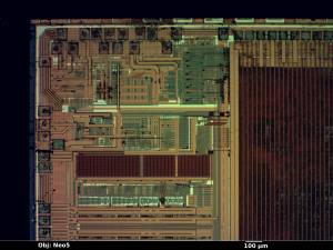
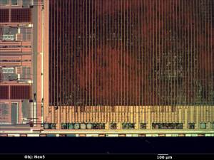
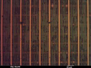
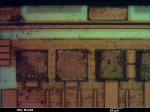
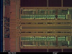
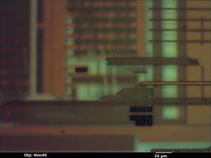
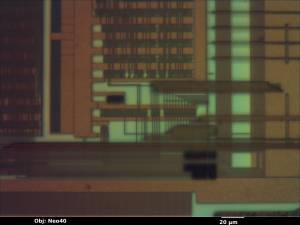
10/100/1000 Ethernet PHY. Process tech looks to be around 180nm with at least five metal layers.

UPDATE: Confirmed by IBIS model (http://www.micrel.com/_Models/IBIS/KSZ9021RN/k9021rn.ibs) to be 150nm TSMC.

Full datasheet from TMSC for the particular I/O cells in use: http://www-afs.secure-endpoints.com/afs/ece/u/blevine/TSMC_IO.pdf

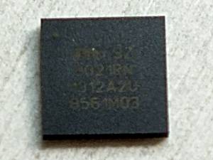
Package

56-pin QFN

dscf4561_cropped.jpg

Die

ksz9021rn_08_bf_neo5x_annotated.jpg

ksz9021rn_09_bf_neo5x_annotated.jpg

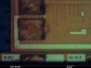
Edge of test pattern in scribe line. Looks like dimensions, possible indicator of 180nm tech? The numbers could be transistor W/L.

ksz9021rn_02_bf_neo40x_annotated.jpg

ksz9021rn_01_bf_neo40x_annotated.jpg

ksz9021rn_07_bf_neo40x_annotated.jpg

ksz9021rn_06_bf_neo40x_annotated.jpg

ksz9021rn_10_bf_neo10x_annotated.jpg

ksz9021rn_03_bf_neo40x_annotated.jpg

ksz9021rn_05_bf_neo40x_annotated.jpg

 
azonenberg/micrel/ksz9021rn.1420169314.txt.gz · Last modified: 2015/01/02 03:28 by azonenberg
 
Except where otherwise noted, content on this wiki is licensed under the following license: CC Attribution 4.0 International
Recent changes RSS feed Donate Powered by PHP Valid XHTML 1.0 Valid CSS Driven by DokuWiki