Table of Contents

Die shots
- Rotated/scaled/roughly aligned images, 16000x14000 each, the dist-*.sh files are the generating scripts
Die shots by John McMaster.
If someone wants to refine the alignement, beware that the vectorization is aligned to the m68000-m-3.png image, which should not change.
Vectorized layers
- Compressed SVG, 42M uncompressed, updated oct 9
The svg uses m68000-m-3.png as background, which should be in the same directory. Beware that inkscape uses 5+G of ram to open and display it.
Six layers with its own style for each: active (blue), polysilicon (red), buried contacts (pink), metal (black), vias (white/grey), capacitors (dark green).
Metal layer was done by Quietust, everything else by me, Olivier Galibert.
Analysis
generate-bitmask-images generate six pbm (bitmap) images (one per layer) using librsvg for the rendering (27M each)
generate-circuit generates the mosfets, the capas, the circuits, etc from the bitmaps. It generates a layers.map file for circuit lookup (2.6G) and a m68000.txt file with the circuit description.
- layers.map and m68000.txt, compressed (8M, expands to 2.8G)
The m68000.txt is a columns-based text file, with the number of entries and the block name at the start of each block. Blocks and columns are:
- circuits (basic elements seen on the die)
- circuit id
- circuit type (a=active, p=poly, m=metal, b=buried, t=transistor gate, c=capacitor)
- net id of which the circuit is part of, net id of the active layer for capas
- net id of the poly layer for capas, -1 for everything else
- x0, y0, x1, y1 coordinates of the bounding rectangle of the circuit, y=0 at bottom (as in inkscape)
- surface of the circuit in pixels
- list of neighbouring (touching) circuits, under the form <type><id> (like b179)
- nets (groups circuits electrically linked together)
- net id
- list of circuits ids (without the types)
- transistors
- transistor id
- circuit id of the gate
- x position of the “center” of the gate
- y position of the “center” of the gate
- net id of one terminal
- net id of the gate
- net id of the other terminal
- length/width ratio of the transistor
Visualisation
- mview, linux/Qt program that displays the circuit and allows interactive simulation
- mplay, linux program that does things with the circuit info (sanity checks, microcode dumping…)
- pins.txt, net naming file
Note that the simulation program is essentially digital, with the side effect that relatively important things like the clock do not work.
The text version of the schematics is composed of 3 parts:
- Header: one line: size x, size y, size ratio w.r.t traced image
- Nodes: one line with the node count followed by one line per node. A node id is its line number, starting at 0.
- Node type, t=nmos enh, d=nmos depl, v=vcc, g=gnd, p=pad, c=capacitor
- x position
- y position
- linked nets ids (t1/gate/t2 for t/d, t for v/g/p, t1/t2 for c)
- w/l ratio for transistors, surface for capacitors
- orientation (except for v/g)
- name
- Nets, one line with the node count followed by one line per net. A net is is its line number, starting at 0.
- Number of reference points in the net drawing (beware, can be 0)
- x, y coordinates of each point, the id of a point is its number, starting at 0
- Number of lines in the net drawing (beware, can be 0)
- pid1, pid2 points ids of the start and end point of each line
- Number of big dots in the net drawing (beware, can be 0)
- points ids of the big dots
- Name of the net, often a number
Schematics
- Google map of the generated schematics, updated oct 9
The schematics are automatically generated from the previously generated files then the circuits are moved around by a lua program. Run remap.lua to generate a new svg/text, run remap.lua toto to also generate the google map tiles.
Schematics analysis
Standard circuits
Latch
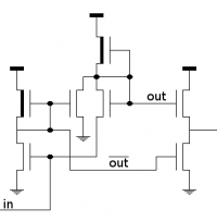
The 68000 uses a *lot* of latches. They generally look like that:
The latch value is set through the input line. The value goes through two inverters then loops through a weak (l/w < 0.2) enhancement mosfet with terminal and gate tied. That way the input drive can easily override it to set a new value.
Both the output and its inverse are available, making it easy to build an amplifier afterwards.
Register bit
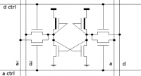
The register bits are described in patent 4,296,469. They look like that:
At the center two inverters are looped to keep the value. Two independant vertical busses a and d are used for both reading and writing. Reading is done by letting the bus float and connecting the memory to the bus with the a ctrl or the d ctrl line. Writing is done by locking a value first on the bus then afterwards connecting the memory bit to the bus.
References
-
- J5H was first silicon, R9M was second

