PCB


Above: LCD screen got a pinprick that allowed mold to grow?
Case front:
naNo
PUPPY


Case back:
Mfg. by
Ying Leung
Intl. Ltd

No.40080
(C) 1997
Playmates Toys
LCD
Dot matrix
Text on screen:
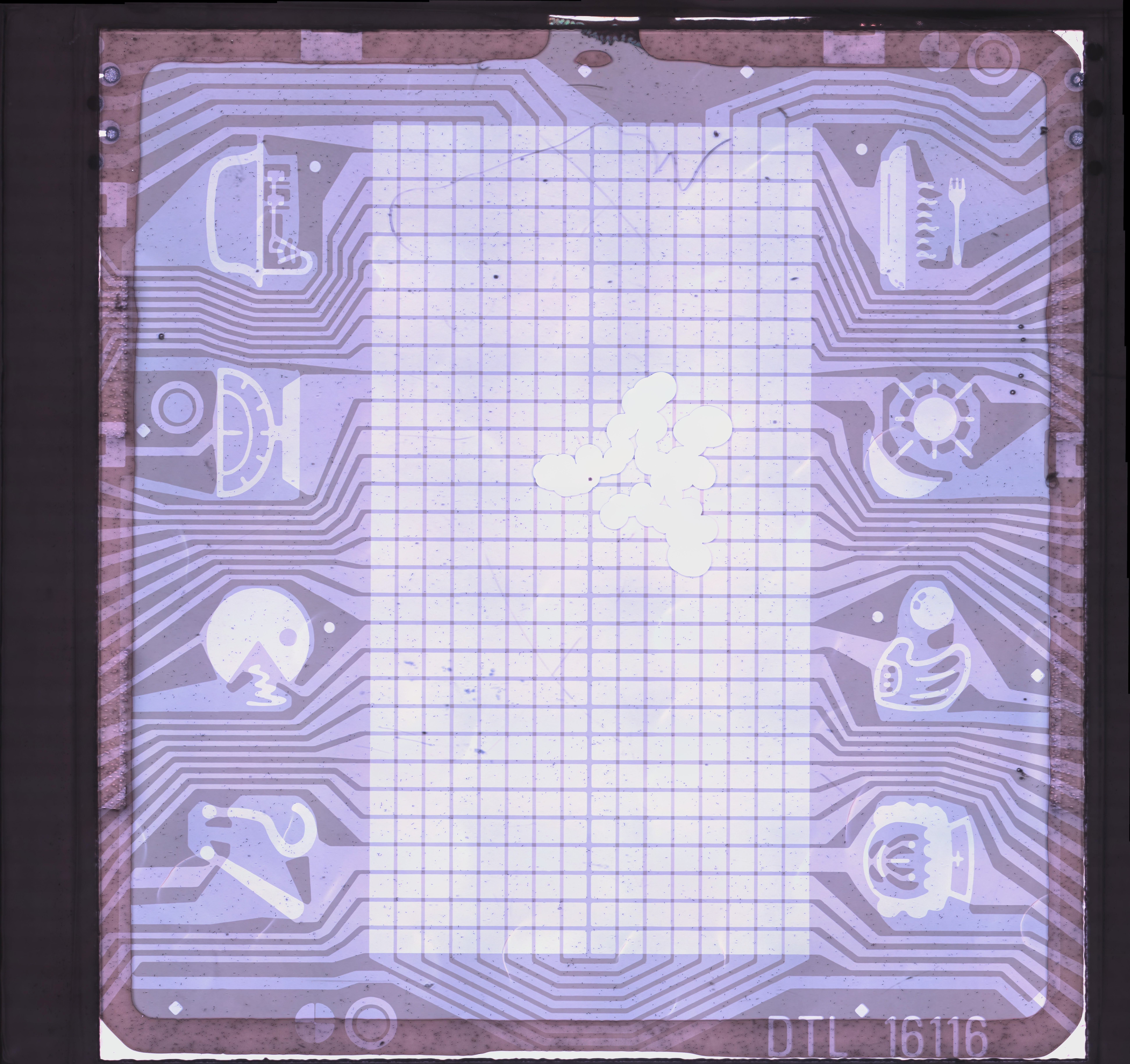
DTL 16116
- Single (7773×7321, 6 MB)
If you use standard brightfield techniques the screen really isn't visible. Usually a voltage is applied to rotate the light and the screen relies on polarizers to make the image dark. Theoretically I could excite the screen and at least see the pixels and considered a few ways to do that. To get the above image I used crossed polarizers and a bright light with the LCD on top of a white surface. The LCD screen is much larger than a normal die so I used my largest usable objective (2x) which has a field of view on the order of 5 mm.
A better setup would be to cross polarizers and shoot through it to a camera. This was just what I had lying around and it was small enough to fit on my microscope stage.
Possibly HDM16116H-2
- Looks to be wrong footprint
- Suggests to use with HD44780
Maybe CRYSTALONICS CDM16116?